Announcement

Collapse
No announcement yet.

โมให้ดีกันเยอะแล้ว มาม๊ะ....มาโมให้"เจ๊ง"กันดีกว่า

Collapse
X
 
  • Filter
  • Time
  • Show
Clear All
new posts

  • จากเลย์เอ้าท์ชุดไฟเลี้ยงของC2จุดนั้น
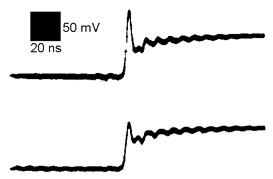
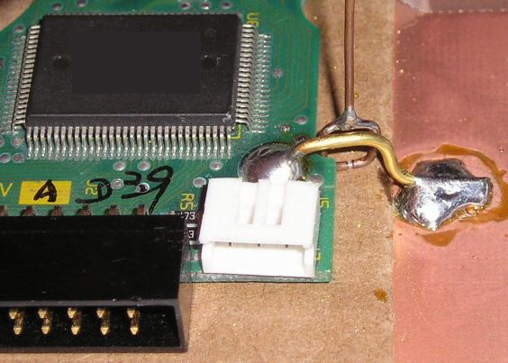
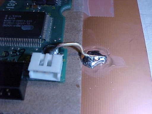
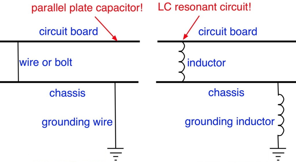
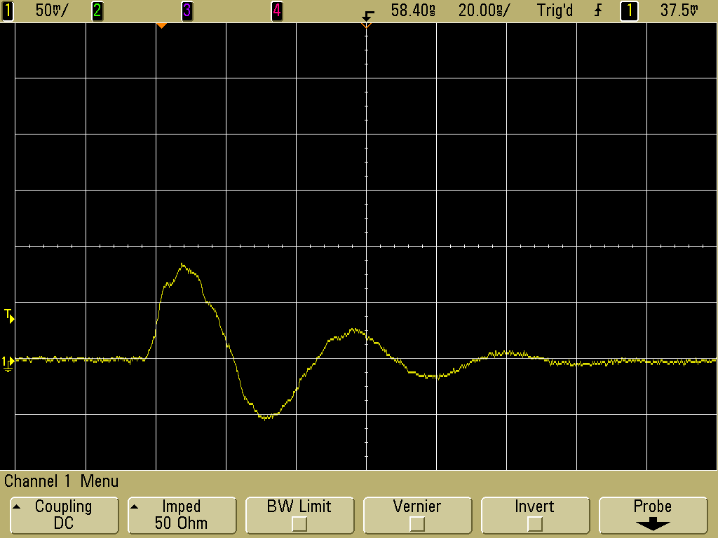
    Cฟิลเตอร์หลัก(ค่าสูง)อยู่ห่.างไปหน่อย บางช่วงลายทองแดงมีการจั๊มลายข้ามชั้นบนชั้นล่าง
    ถ้าไม่ใช้ค่า0.1uFจะใช้ค่า1uF เพื่อชดเชยเส้นทางของลายทองแดงก็ได้ครับ ถ้ามือนิ่งพอก็บัดกรีขาCที่ขา1798เลยครับ

    จริงๆอยากแนะนำให้ใช้1uFน่ะ ถ้าใช้ของEROได้ก็ดี เพื่อชดเชยเสียงบางอย่างของตระกูลburr-brown
    (ความเห็นส่วนตัว -- ถ้าหาSprague Silver Micaรุ่นเก่าๆได้ และไม่สนใจเรื่องขนาดที่มันใหญ่โตมโหฬารก็น่าลองดู
    เหมือนกัน)


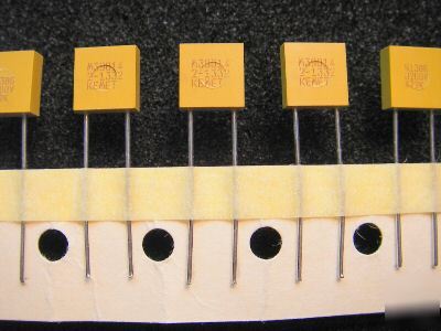
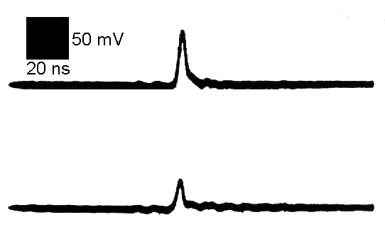
    ถ้าจะเน้นตัวเล็กๆแต่ทำงานได้ตรงตามหน้าที่ก็ใช้ชนิดMultilayer Ceramic Capacitorก็ได้ รูปร่างกับขนาดก็คล้ายๆvishay vshครับ


    เกรดดีหน่อย (Low inductance and undetectable ESR) ก็หน้าตาแบบนี้


    -------------------------------------------


    Rรุ่นนี้ก็ใช้ได้ครับ แต่ควรใช้แบบตัวเดียว หลีกเลี่ยงการต่อแบบอนุกรมหรือขนาน
    vishayรุ่นนี้เสียงจะบางหน่อย
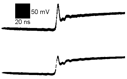
    Last edited by keang; 27 Apr 2012, 09:56:21.

    Comment


    • เครดิต : Douglas C. Smith
      > High Frequency Measurements Web Page


      February 2000 : Measuring Capacitor Self-inductance and ESR

      Figure 1. Test Circuit for Measurement of Capacitor Self-inductance and ESR


      Technical Background
      The parasitic parameters of a capacitor, that is its equivalent series resistance (ESR) and its inductance, affect the way the capacitor performs in circuits. Some applications are very sensitive to these parameters. For instance, a bypass capacitor used between power and ground in a digital circuit must be able to supply current quickly to nearby active devices. If it has too much inductance it will not be able to do this. Similarly, the transient response of a capacitor used to divert a current pulse due to electrostatic discharge is very important to the ability of the capacitor to do its job.

      So how can the parasitic parameters of a capacitor be measured? One could certainly connect the capacitor to a network analyzer and get a very good characterization. Such an instrument can be quite expensive though. Even the less expensive capacitance measuring instruments may not be available when needed. Both instruments may not provide the information in an easily usable form. If you have a pulse generator (preferably with a 50 Ohm output impedance) and an oscilloscope, you can easily measure the transient response of a capacitor. From this data the capacitor's ESR and inductance can be determined.

      First, construct the simple network shown in Figure 1 at the end of a 50 Ohm coaxial cable fed from a 50 Ohm pulse generator. A 50 Ohm resistor is used in Figure 1 to terminate the coax during the rising edge and provide a total of 100 Ohms of source impedance. The resistor shown is a 51 Ohm 1/2 watt carbon composition resistor with one lead trimmed so that the resistor just seats with the trimmed lead fully inserted into the BNC connector. It may be necessary to put a little solder bump on the resistor lead so that it stays firmly in the BNC connector. The capacitor to be tested is connected between the end of the resistor and the shell of the BNC connector. An oscilloscope is connected directly across the capacitor using leads as short as possible to connect the probe. Probes with a resistive input impedance of 500 to 1000 Ohms are recommended. Standard 10X "Hi-Z" probes often have rising edge effects that will distort the part of the waveform used for the calculations.


      .... ตัดเนื้อหาส่วนของการคำนวนออก แต่ควรเข้าไปอ่านเนื้อหาทั้งหมด ....


      Figure 3 below shows the initial rise from the generator. The black square indicates the vertical voltage and horizontal time scales. The open circuit voltage was a little over 4 Volts with about a 5 nanosecond risetime. The data in Figures 3 through 6 were taken with an analog scope some years ago. Figures 4 through 6 show data obtained from several leaded capacitors (as opposed to surface mount). Two traces were taken for each capacitor. The lower trace was measured at the capacitor body where the leads entered and the upper trace included the minimum amount of lead to practically connect the capacitor to a printed wiring board. The upper trace would not be needed for modern surface mount capacitors unless one wanted to model the connection inductance from the capacitor to the point of interest on a printed wiring board.

      Figure 3. Input From Pulse Generator


      Figure 4 shows data from a 4 uF electrolytic capacitor. The ESR offset is about 50 mV yielding an estimate of the ESR of just over one Ohm. Notice that there appears to be some oscillations on the 1/C part of the slope. This could be scope probe resonance or a resonance in the capacitor. The data was taken with a standard 10X Hi-Z probe, so the probe is suspect. I have seen capacitors with pronounced oscillation from internal resonance. If you are planning to put a large capacitor in parallel with a smaller one, especially if they are constructed from different technologies, it would a good idea to check out the impulse response of the combination using this method. It is possible for the smaller capacitor to resonate with the inductance of the larger one, causing an unexpected result.

      Figure 4. 4uF Capacitor


      Figure 5 shows the result for a 1 uF capacitor of the same construction as the 4 uF capacitor tested in Figure 4. Note that the inductance is similar to the 4 uF capacitor, but the ESR is slightly lower. Since an analog scope was used, the waveform was repetitive and the slight slope on the left half of the waveform was the end of the exponential fall from 5 volts. If a single pulse on a digital scope was used, the slope to the left of the Ldi/dt spike would be zero.

      Figure 5. 1uF Capacitor


      Figure 6 shows the result for a 1 uF radial ceramic capacitor (square case). Note the low inductance and undetectable ESR. Note also that the slope of the 1/C exponential rise is flatter indicating more capacitance than the 1 uF capacitor of Figure 5. This may be due to the fact that the electrolytic capacitor used for Figure 5 may have lower capacitance near zero voltage than at its operating voltage whereas the ceramic capacitor has a more constant capacitance with voltage. The inductance corresponding to the lower trace is estimated to be 4.4 nH.

      Figure 6. 1uF Ceramic Capacitor


      It is interesting to note that a 0.1 uF ceramic capacitor in the same size package as the 1 uF of Figure 6 showed a slightly higher inductance in this test setup. I believe this was due to the fact that the smaller capacitor did not fill the package and internal lead inductance caused the effect. In this case, a 1 uF capacitor was a better choice than a 0.1 uF!

      One of the advantages of this test is that the output waveform is the transient response of the capacitor. The voltages developed across the capacitor in this test are directly related to what will happen in a real circuit if the current risetime from the generator is similar to what the capacitor will see in its intended application.


      --------------------------------------------------------


      December 2011 : Measuring the Resonant Frequencies Of Heat Sink Tines

      ( Your heat sink can be the source of high frequency EMC emissions! )

      Figure 1. Typical Heat Sink


      Abstract :
      Heat sinks on ICs can be a source of emissions at high frequencies in the multi-GHz range. A method of identifying high risk frequencies by measuring the resonant frequencies of the heat sink tines is discussed.

      Discussion :
      Many heat sinks have tines that protrude perpendicularly from a base plate such as the one shown in Figure 1. Today's clock frequencies are so high as to be able to excite the tines as quarter wave monopoles resulting in something like an antenna farm on top of the IC, potentially radiating a clock harmonic or other source resulting in an emissions problem.

      One way to measure the resonant frequency of physical structures in general and heat sink tines in particular is shown in the June 2006 Technical Tidbit, Measuring Structural Resonances on this site. Basically, one would hold a very small shielded loop at the base of one of the heat sink tines to couple energy into the tine. By measuring the reflected signal from the small shielded loop, the resonant frequency of a tine can be measured as the frequency where the reflected signal experiences a dip as the tine absorbs energy from the loop. The lowest frequency this would occur at is the frequency at which the tine is 1/4 wavelength. The method is described in detail in the June 2006 article referenced above. Figure 2 shows the method being applied to a PCB test board mounted over a copper clad board. The object in that case is to measure the resonant frequency of the LC tuned circuit composed of the capacitor formed by the PCB and copper clad board, and the inductance of the short wire between them.

      Figure 2. Use of a Small Shielded Magnetic Loop to Measure PCB-Chassis Resonance


      I observed a case some years ago where 4.7 GHz was leaking out of every slot and seam in the enclosure of a product. It turned out that 4.7 GHz was the third harmonic of the processor clock. When I measured the resonant frequency of the hea tsink tines, the dip in the reflection from the loop was right at 4.7 GHz indicating the tines were 1/4 wavelength monopoles, very efficient radiators, at that frequency. If the tines had been longer or shorter the emissions problem would have been reduced significantly.

      Summary :
      Using the simple method outlined, one can determine the resonant frequencies of the tines on a heat sink. Knowing this information in combination with information about the IC used allows an assessment of the risk of emissions problems from the heat sink.


      --------------------------------------------------------


      September 2011 : PCB-Chassis Ground Connections - Avoiding Pitfalls Due to Unintended System Resonances

      Figure 1. PCB With Chassis Ground Connection


      Abstract :
      PCB to chassis ground connections are often needed in electronic equipment, but if care is not taken, the PCB and the chassis ground structure can become a hi-Q resonant circuit that may cause problems. Background information is given and techniques to avoid problems in designs are discussed.

      Discussion :
      Connecting PCB signal grounds to equipment chassis ground is a common feature in electronic systems although not necessarily done as shown for the experimental board in Figure 1. Problems can arise when the PCB and nearby metal, whether it is another PCB or chassis metal, form a parallel plate capacitor and the connections between them form an inductor. The combination forms a high-Q resonant circuit as illustrated in Figure 2. If this resonant circuit is tuned to a clock harmonic or other critical system frequeny, there is a risk of an EMC problem or even an operational problem for sensitive circuits. At today's frequencies, all PCBs have significant capacitance to nearby metal and all connecting wires are inductors.

      Figure 2. Equivalent Circuit of PCB and Chassis Connections


      Summary :
      Don't take chances with your design, engineer the system resonances involving PCBs rather than letting system performance fall to chance.


      --------------------------------------------------------


      July 2011 : Measuring ESD Stress on a PCB
      ( When Conventional Measurements Don't Work )

      Figure 1. Measured Current Through a Protection Device on a PCB
      ( Vertical Scale = 50 mA/div, Horizontal Scale = 20 ns/div )


      Abstract :
      Measuring voltage stress on components on a PCB under ESD conditions can be difficult as the ESD noise can inject error in the measurement. Often this error is larger than the voltage of the stress to be measured. A method of measuring voltage stress is discussed that has very high common mode rejection and low ESD induced error.

      Discussion :
      ESD induced error makes accurately measuring voltage stresses on a PCB difficult. In addition to high common mode noise, high amplitude time varying electric and magnetic fields can introduce error in the measurement loop formed by the voltage probe and the nodes to be measured unless this loop is kept very small. One way to accurately measure high frequency voltage stress is to replace the component that is being stressed, such as an IC, with a TVS or similar protector connected across the two nodes to be measured. In series with the protector, form a loop as small as possible to insert a current probe to measure the current through the protector.

      As the ESD or other pulsed voltage stress is increased, an increase in current through the parasitic capacitance of the protector will be seen that follows the stress applied. When the breakdown voltage of the protector is reached, additional increase in current may be noted and the waveform will quickly show the current waveform as the stress is increased further for a protector that clamps to a specified value. For a protector that latches to nearly a short after turn-on, like an SCR, the current at the point of latching will be seen. Figure 1 shows the current through a protector that clamps to a specified voltage in a circuit with applied stress from a Fischer Custom Communications model TG-EFT high voltage pulser. The protector capacitance is helping form a resonant response with circuit inductance. The current waveform reaches a peak of about 80 mA.

      In Figure 2, the stress is doubled and the peak current reaches about 150-160 mA, approximately increasing linearly with applied stress and keeping the same waveshape except the ringing frequency is slightly higher.

      Figure 2. Measured Current Through Protection Device on a PCB at 2X Applied Stress
      ( Vertical Scale = 50 mA/div, Horizontal Scale = 20 ns/div )


      For Figure 3, the stress is increased to 3X the value in Figure 1. Note that the waveshape is beginning to change although the peak current is about 3X of the current in Figure 1, about 230 mA.

      Figure 3. Measured Current Through Protection Device on a PCB at 3X Applied Stress
      ( Vertical Scale = 50 mA/div, Horizontal Scale = 20 ns/div )


      In Figure 4, the stress is increased to 4X the value in Figure 1. Now the waveshape is definitely changed and is beginning to look like the current waveform I expect at this point in the circuit. The peak current is now almost 300 mA.

      Figure 4. Measured Current Through Protection Device on a PCB at 4X Applied Stress
      ( Vertical Scale = 50 mA/div, Horizontal Scale = 20 ns/div )


      The stress that just begins to breakdown the protector is that of Figure 3 where the waveshape begins to change. Note that we are not trying to accurately measure the current, so some electric field response of the current probe is acceptable, we are looking for a change in the waveshape of the current as the stress increases. The current probe should be as small as possible so as to minimize the loop needed to insert it into the circuit.

      The lower capacitance the protector has before breakdown, the larger the difference in amplitude and waveshape will be noted at the point of breakdown. Also, if the capacitance of the protector is much larger than the original device it replaced, the capacitance may reduce the voltage across the protector resulting in a larger applied stress being required to breakdown the protector. This will result in measurement error that will understate the stress on the original device to be measured. In general, the lower capacitance the protector has the better, but for sure it should not be much larger than the original device it replaces in the circuit.

      Summary :
      Using a current probe and a protector connected in place of a device on a PCB to measure voltage stress on the device is a useful way to minimize error from sources like ESD in the voltage stress measurement. The capacitance of the protector used should be minimized and be on the order of the original device capactiance. The loop formed for the current probe should be as small as possible.


      --------------------------------------------------------


      August 2009 : The Square Shielded Loop - Part 6, Measurements in the Time Domain Using a Comb Generator
      ( An unusual use for a comb generator )

      Figure 1. A Shielded Loop Being Used to Sense Signal Current from a Comb Generator


      Abstract :
      Possible sensitivity to electric fields/capacitive pickup has been a factor in the past in selecting shielded magnetic loops over unshielded ones. Data is presented to show that in the near field, shielded loops may be required for sensing signal currents in some cases. Data presented in prior Technical Tidbits have shown the opposite to be true for other cases.

      Discussion :
      Figure 1 shows a shielded magnetic loop probe held near a ground plane split to sense signal current. Probe construction is shown in the cutaway view of Figure 2. A section of semi-rigid coax is shorted at it's end and then bent around and the shorted end is soldered onto the coax to make a loop. A small gap is cut in the shield to permit the loop to be sensitive to magnetic fields. In Figure 2, the shield gap can be seen at the midpoint of the rightmost side of the loop, opposite the soldered junction.

      Figure 2. Construction of a Square Shielded Loop


      Data was also taken using the unshielded wire loop shown in Figure 3 to compare the responses of the two magnetic loops and determine when the wire loop's electric field sensitivity becomes important.

      Figure 3. A Simple Wire Loop


      The signal source, shown in Figure 4, for this experiment was an AET USB Powered Comb Generator. Comb generators produce a large number of harmonics that are useful in a number of frequency domain measurements normally made using a spectrum analyzer or similar instrument. But in this case, it was used to furnish fast pulses for the experiment and measurements were made on an oscilloscope. The comb generator used has a 1.8 MHz fundamental frequency and edge rates of about 400 picoseconds.

      The output of the comb generator was connected to the BNC connector in the upper left corner of the circuit board in Figure 1. The resulting current in the signal path and the load resistor on the right side of the board resulted in signal current flowing around the split in the ground plane and both shielded and unshielded loops were used to sense this current.

      Figure 4. AET USB Powered USB Comb Generator


      Figure 5 shows the test setup using the simple wire loop of Figure 3. This is the same setup shown in Figure 1 for the shielded loop except for the use of the unshielded loop.

      Figure 5. Test setup with unshielded wire loop


      Figure 6 shows the output of the shielded loop. A resonance at about one GHz can be seen on the waveform. This could be partially due to loop self resonance or capacitive coupling to the shield. To test the effects of electric field coupling, the loop was rotated by 180 degrees. The inductive pickup should invert and any capacitive pickup should stay nearly the same. The reversed loop output is shown in Figure 7 and is just an inverted version of the wave shape in Figure 6. Since the waveforms in Figure 6 and Figure 7 are inverted with otherwise the same shape, capacitive coupling to the loop is not significant for this configuration.

      Figure 6. Output from shielded loop
      ( vertical scale = 10 mV/div, horizontal scale = 2 ns/div )


      Figure 7. Output from shielded loop - reversed orientation
      ( vertical scale = 10 mV/div, horizontal scale = 2 ns/div )


      Figures 8 and 9 show the same cases for the unshielded wire loop. One can easily see these waveforms are not just inverted versions of each other. There is significant capacitive coupling between the loop and the circuit. The capacitive coupling combined with the inductance of the wire probably produced the lower frequency resonance easily seen in Figure 9 and to a lesser extend in Figure 8.

      Figure 8. Output from wire loop
      ( vertical scale = 10 mV/div, horizontal scale = 2 ns/div )


      Figure 9. Output from wire loop - reversed orientation
      (vertical scale = 10 mV/div, horizontal scale = 2 ns/div)


      I encourage you to read the other five Technical Tidbits in the "Square Shielded Loop" series. These are linked just below the summary paragraph. In the September 2008 Technical Tidbit, "The Square Shielded Loop - Part 5," the unshielded wire loop was used for signal injection of pulses with a 2 ns edge rate. A significant capacitive effect was not present. If fact, for injecting signals into the board of Figure 1 over the ground split parallel to the signal path, the simple wire loop worked better than the shielded loop, having a flatter frequency response. In that case, the shield of the loop formed a parasitic resonant circuit with the circuit board that affected the frequency response of the coupling from the loop to the board.

      Summary :
      Significant capacitive coupling was demonstrated when using an unshielded wire loop to sense current flowing near a ground plane split. Yet, other Technical Tidbits in the "Square Shielded Loop" series show that for injecting a signal into a signal path crossing a ground break, the simple wire loop was superior. Until more work is done, one must test to see which type of loop works best for a given situation and not just assume that one type of loop is always better.


      --------------------------------------------------------


      April 2010 : Identifying Switching Power Supply Noise in Systems
      ( Frequency Domain Measurements )

      Figure 1. Test Setup For Measuring Switching Power Supply Induced Noise Current into a Nearby Wire
      ( Spectrum Analyzer Screen at 10 dB/div Vertically and 10 MHz/div Horizontally )


      Abstract :
      Switched mode power supplies can generate significant harmonics of such an amplitude as to cause EMC emissions problems in the 30 to 100 MHz range and occasionally at higher frequencies. Identifying switching power supply noise is discussed as well as one coupling method that can result in excess radiated emissions.

      Discussion :
      Figure 1 shows the test setup used to generate the data. The setup is composed of a switching power supply, a (black) wire draped across the supply, an Agilent N9320B spectrum analyzer, and an Fischer F-33-1 current probe. The power supply is powering a 48 Watt, 12 Volt incandescent light bulb through the yellow test leads. The black wire passing through the F-33-1 current probe is about three meters long and its center has been positioned over the power supply. The plot on the analyzer screen in Figure 1 extends from zero Hz to 100 MHz at 10 MHz/div.

      The noise floor on the screen of the analyzer is about 30 dBuV, a level that corresponds to enough current flowing in a one half wavelength dipole antenna to just hit the CISPR/FCC class B emissions limits in the 30 to 100 MHz frequency range. You can see the level of current near 40 MHz is about 20 dB above that level and could cause a Class B emissions problem. In reality, the power supply exhibits broad band noise, but the current in the wire peaks at the frequency at which the wire is a one half wavelength dipole. At that frequency, the driving point impedance of a dipole is near 70 Ohms, its minimum value, and the induced voltage from the power supply in the black wire is able to produce a current maximum at the center the wire.

      The local field from the power supply is probably not physically large enough to radiate efficiently at 40 MHz, but once it induces enough current in the nearby black wire, the wire itself is long enough to be an efficient radiator. That is what has happened in this case.

      We know that the source is the power supply for this simple case, but in some cases the source might not be so obvious. One way to discover if a broadband noise, such as shown on the analyzer screen in Figure 1, is due to a switching power supply is to adjust the analyzer as shown in Figure 2.

      Figure 2. Spectrum Analyzer Screen Centered at 43.5 MHz with a 100 kHz/div Horixontal Scale and a Resolution Bandwidth of 1 kHz


      The analyzer has been adjusted in Figure 2 to focus the plot around a center frequency of 43.5 MHz with a frequency span of only one MHz, 100 kHz/div. The resolution bandwidth has also been lowered from 100 kHz in Figure 1 down to one kHz, a value consistent with the horizontal scale of 100 kHz/div. With these analyzer parameters, you can clearly see peaks in Figure 2 separated by about 120 kHz, the fundamental frequency of the switching power supply used for this experiment.

      Noise originating in switching power supplies that operate at a constant frequency will produce a spectrum plot similar to Figure 2, although the spacing of the harmonics may be different. That the noise is actually coming from a specific supply can be determined by holding a small loop probe near the power supply to pick up induced noise. Display the loop output on an oscilloscope or spectrum analyzer to determine the fundamental frequency. If the observed noise has a harmonic spacing the same as the fundamental switching frequency of the power supply, the supply is the likely source of the noise unless there are other supplies in the system with "the same" fundamental frequency. For the case where there are several power supplies with "the same" fundamental frequency, they are likely slightly different and this information can be used to narrow the source of the noise down to one supply out of several.

      Summary :
      By expanding the spectrum plot of a broadband noise, individual harmonics from the source of the noise can be resolved. In many cases, the spacing of harmonics on the expanded plot will identify a switching power supply as the source of the noise.
      Last edited by keang; 27 Apr 2012, 11:34:34.

      Comment


      • ซ่อม x-fi forteให้ ใช้ได้แล้ว
        จัดหม้อแปลง+linear reg ให้opampมันเลย

        กำลังร้องเพลงอยู่ ดีใจมากมาย
        รูปเดี๊ยวมาเอาลงครับ

        Comment


        • โหลดโหดนิหนึ่ง
          auzentech x-fi forte

          ปัญหาของตัวการ์ด
          ตอนได้การ์ดมาเลย เจ้าของเก่าบอกใช้ๆ ไปแล้วมีเสียงตุ๊บๆ หลุดมา
          เช็คอาการตามเจ้าของเดิมบอกเสร็จก็เสียบดองทิ้งไว้อยู่นาน
          จนวันหนึ่งลองเปิด ปรากฎเสียงออกมาเบามากๆ
          ไล่เช็ควงจรกันพักใหญ่ ก็เดาแถๆ ว่าภาคจ่ายไฟเสีย

          --------

          โล๊ะภาคจ่ายไฟสวิทชิ่งของเก่าทิ้ง +เปลี่ยน c liquid elec. ของเก่านิดหน่อย


          จั้มสาย ต่อไฟเพิ่ม เอาไปใกล้ๆ ขาopamp เลย

          กะความยาวพลาดไปหน่อย ออกมาไม่ค่อยสวย

          เอาประสิทธิภาพกว่านี้ คงเอาic reg.มาแปะที่ขาเลย แต่ต้องแก้ปัญหาเรื่องพื้นที่ให้ได้(+พื้นที่ซิงค์มันด้วย ค่อนข้างร้อน)

          มาดูในรูปถึงเห็นว่ามันยังไม่สะอาดมีคราบ บางทีมองตาเปล่าลำบาก ถ่ายรูปแล้วมันสะท้อนแสงออกมามองง่ายกว่า


          ac to dc adaptot ที่ใช้จ่ายไฟ +-12ให้ opamp
          ใช้kit ของประกิต มี nichicon HE ติดมากับkitเลย
          7912ใช้ของon 7812ใช้ของti ซิงค์ซื้อเพิ่ม แล้วหาทางยัดมันลง(ต้องรองไมก้า+bush เดี๊ยวช้อตกันเองระหว่าง7912กับ7812)
          หม้อแปลง12 0 12 Vac 2A henry ออกจะเหลือเฟือไปหน่อย เพราะยังไงก็ไปตัน1Aที่diode กับ ic reg. แต่ก็เพื่อไปก่อน หม้อแปลงจะได้ไม่ร้อนมากเวลาทำงาน

          การทำงาน ตอนนี้ก็ร้องเพลงได้ปรกติ ทั้ง ต่อดิจิตอลเอาท์ อนาล็อคเอาท์

          เว้น แจ็คหูฟัง มีปัญหาหน่อย มีความถี่สูง ดัง"วี๊"เบาๆ หลุดมา เป็นมาตั้งแต่ก่อนซ่อมแล้ว ตอนแรกคิดว่ามาจากภาคจ่ายไฟสวิทชิ่งบนบอร์ด
          สงสัยเป็นเพราะอย่างอื่น ตามหากันต่อไป

          เรื่องเสียงรอเบิร์น แต่ดองไว้นานแล้วจำเสียงเดิมไม่ได้สนิทดี
          อะไหล่บ้างจุดก็ยังไม่ได้คัดมาก แค่เอามาลองให้มันซ่อมได้ก่อน


          ---

          เอามาอยู่ด้วยกันได้อ่านง่ายๆ

          updateเช่นกัน
          x-fi forte น่าจะเจอต้นตอ ของแจ็คหูฟัง แจ็คมันไม่แน่น ขยับไปบางมุม แล้ว noiseหายเลย ขยับอีกมุมมันก็กลับ

          ต่อแจ็คหูฟัง สุ่มเสียงใช้ได้ แนวเสียง ออกกว่าเรียบๆหน่อย ไม่ได้ไปดันเสียงบางเสียงขึ้นมาให้ดูเด่น เหมือนsound creative บางตัว
          รอเบิร์นต่อไป
          แต่กำลังขับ ยังไงก็แพ้ชุดแอมป์แยก (อาจจะเพราะโวลุ่มกับgain ในตัวมันเร่งได้แค่นั้นด้วย)
          เร่งสุด แล้วก็ยังดังไม่เท่าชุดdac-ampที่ใช้อยู่ + จุดที่เร่งไม่สุด deep bass หูยังไม่ค่อยจะสั่น ทั้งทีเบสบางช่วงมีมากกว่าชุดแยกอีก(แต่ก็นั้นแหล่ะอาจจะเป็นแค่บุคคลิกมันก็ได้ ไม่ใช่กำลังขับมันไม่พอ)
          Last edited by ManiacMaew; 29 Apr 2012, 16:35:27.

          Comment


          • หาสาย Canare 4S11 กับ 4S8 มา 2 วันแล้ว ไม่เจอเลย -*- ตอนไม่อยากใด้ล่ะเต็มไปหมด

            มีเรื่องมารบกวนหน่อยครับ

            คืออยากใด้ดอกทวิสเตอร์โดมผ้าแบบถูกๆ คุณภาพไช้ใด้สักคู่ เอามายัดตู้ sat เดิม พอจะหาแถวใหนใด้บ้าง ?

            ( ถ้าใด้แบบเดียวกับ Solo6 ล่ะแจ่มเลย ผมชอบแนวนั้น )

            แล้วดอกทวิสเตอร์โดมผ้า ไช้ C คร่อมเฉยๆ เหมือนทวิสเตอร์โดมพลาสติกใหมครับ ?

            เคยซ่อมหัวเสียบลำโพง sat ของ Klipsch GMX เห็นไช้ C คร่อมเอาง่ายๆเลย ( แพงซะเปล่า -*- ) แต่โดมผ้านี่เห็นไช้ network ตลอด

            Comment


            • ทวิสเตอร์ไม่ลองไปหา npe ของ Hokutone อ่ะครับ ราคาไม่แพงด้วย ดอกล่ะ 1xx กว่าบาท มีให้เลือกหลายโดมด้วยครับ

              Comment


              • Update
                X-fi ที่ผมโมผมยังอยู่ครับตอนนี้ยังไม่พัง หาพัดลมเป่าแล้วครับเป่ามันทั้งการด์เลยครับ

                Comment


                • updateเช่นกัน
                  อ่านได้ในท้ายโพสต์เดิม
                  http://www.overclockzone.com/forums/...1#post40598754

                  --------

                  สงสัยหูผมจะไม่ชอบcreative asio output ใช้ยังไงก็ไม่ โอเค แต่มันมีข้อดีที่ว่าเวลาใช้analog out+ aduio creation mode มันสลับsampling rateให้เอง
                  (digital out ใช้wasapi outout ก็ยังสลับให้เองอยู่)

                  เวลาสลับsampling rate ก็จะสะดุดเป็นเสียงซ่าๆ นิดหนึ่งก่อนขึ้นเพลง
                  Last edited by ManiacMaew; 29 Apr 2012, 16:34:57.

                  Comment


                  • C10, C11, C19 คาปา 3 ตัวนี้จำเป็นต้องเปลี่ยนด้วยไหมครับ

                    Pin 28 VCC2L Analog power supply (L-channel DACFF), 5 V
                    Pin 23 VCC1 Analog power supply, 5 V
                    Pin 15 VCC2R Analog power supply (R-cahnnel DACFF), 5 V

                    capa.jpg

                    pcm1798.jpg

                    ส่วนนี่รูปตัวอย่างที่มีการโม เอามาให้ดูกัน

                    201203_24_59_c0021859_6314857.jpg
                    Last edited by b_amnart; 29 Apr 2012, 19:49:53.

                    Comment


                    • ^^^
                      -c10 c19 น่าเปลี่ยนน่ะ ถ้ามีพื้นที่พอ

                      - อ่านแล้ว งงหน่อยๆ
                      รูปโมที่เอามาให้ดูนี้รูปที่โมเอง หรือตัวอย่างที่เอามาดูเฉยๆ


                      -ลองดู c48 กับ c20
                      http://pdf1.alldatasheet.com/datashe.../MC33079D.html

                      ในภาพเห็นตำแหน่งชัดเลย


                      พื้นที่มีจำกัด ก่อนทำจริงก็ลองคิดดูก่อนว่าจะทำจุดไหนบ้าง
                      Last edited by ManiacMaew; 29 Apr 2012, 18:57:19.

                      Comment


                      • Originally posted by ManiacMaew View Post
                        ^^^
                        -c10 c19 น่าเปลี่ยนน่ะ ถ้ามีพื้นที่พอ

                        - อ่านแล้ว งงหน่อยๆ
                        รูปโมที่เอามาให้ดูนี้รูปที่โมเอง หรือตัวอย่างที่เอามาดูเฉยๆ


                        -ลองดู c48 กับ c20
                        http://pdf1.alldatasheet.com/datashe.../MC33079D.html

                        ในภาพเห็นตำแหน่งชัดเลย


                        พื้นที่มีจำกัด ก่อนทำจริงก็ลองคิดดูก่อนว่าจะทำจุดไหนบ้าง
                        ขอบคุณครับ รูปตัวอย่างเอามาให้ดูกันนะ พื้นที่จำกัดจริงๆ ถ้าเปลี่ยนคงใช้พวก Ceramic Multilayer ตัวเล็กๆเอาครับ
                        ส่วนภาพที่ทำเครื่องหมายไว้เป็นตัวจริงของผมที่ทำความสะอาดแล้วถ่ายไว้ตอนเช็ควงจร
                        Last edited by b_amnart; 29 Apr 2012, 19:58:45.

                        Comment


                        • ใช้ out put อะไรเป็นหลักเหรอครับ rca หรือ 6.35 ของหูฟัง
                          Last edited by ManiacMaew; 29 Apr 2012, 21:28:27.

                          Comment


                          • Originally posted by ManiacMaew View Post
                            ใช้ out put อะไรเป็นหลักเหรอครับ rca หรือ 6.35 ของหูฟัง
                            ใช้ out put rca เป็นหลักจะเอาไปแทนที่ xonar dx ครับ

                            Comment


                            • ลองทำทีละสเตปครับ เสียเวลาหน่อย แต่เราจะรู้ว่า อะหลั่ยที่เราใส่เข้าไปมันตอบโจทย์ได้ตรงใจเรารึเปล่า หรือ เหมาะกับเราไม๊
                              - ถ้ามันให้เสียงได้ถูกใจเรา ค่อยมาเปลี่ยนที่3จุดใหม่ที่พูดถึงครับ
                              - ถ้ามันให้เสียงไม่ถูกใจ ก็ลองหาตัวอื่นมาลองใหม่

                              - 3จุดใหม่ที่ถามก็ทำหน้าที่ไบแคปเหมือนเดิม
                              - C10, C11, C19, C26 เค้าให้ใส่ใกล้กับขา1798มากที่สุด
                              Last edited by keang; 29 Apr 2012, 22:23:03.

                              Comment


                              • เรื่องเกี่ยวกับ c ลองไปอ่านกัน
                                ตัวใหญ่หน่อยได้อ่านง่าย

                                Applications Notes:

                                Capacitor "Self Inductance"

                                The inductance of a practical capacitor limits the frequency range that it can be used for. At some frequency, the inductance of the capacitor will form a series resonant circuit. At this frequency the capacitor is useless as a filter. The series inductance of the capacitor also raises the impedance, limiting its ability to pass AC current. For this reason, DC power supplies often use a parallel combination of capacitors. For low frequency filtering (60-120Hz) a large value of capacitance is necessary. A polar electrolytic of several hundred to several thousand microfarads is the common choice. The large series inductance of this capacitor makes it effective only up to several hundred kilohertz. Above this, the high impedance makes it appear as "not there" to higher frequency components. To extend the frequency range, a small tantalum cap (several uF) is often added. This has much lower series inductance, so it is effective up to the low megahertz. The value can be small, because the lower frequencies are being filtered effectively by the large electrolytic. At even higher frequencies, a small ceramic (.01 to .1uF) is added in series. The same rules apply, the cap can be even smaller because the frequency of interest is even higher. Ceramic caps for decoupling use can be almost any variety (X7R, Z5U etc.) This will make a power supply filter that performs equally well at eliminating AC line hum, radio stations, microprocessor noise, etc. Remember, the filter not only stops noise from riding into your circuit, it stops your noise from reaching other circuits (yours, your neighbors' etc).

                                The length of traces and wire that separate individual components on a printed circuit board or a system also have "series inductance". This means that if there is a sudden, local demand for current, the voltage at that point in the circuit will drop until the current flow makes it through the current limiting inductance. For this reason, capacitors are placed very near the power terminals of active components. This limits the series inductance, so a small capacitor can act as a filter for local noise, as well as a small current reservoir. These are known as decoupling capacitors, because the make the local node act independently of (or decoupled from) the rest of the circuit. The inductance of the wiring is usually small, so the main electrolytic filter caps are still able to handle the low frequencies. At the chip level, a small tantalum or electrolytic (1-10uF) in series with a ceramic (.01-.1uF) is usually more than enough. Lack of decoupling can cause circuits to perform badly or sometimes, not to work at all. The opposite of decoupling is "coupling", meaning that there are unintended connections and interactions between circuit functions.

                                Coupling Capacitors: Capacitors are often used to block different DC voltages in successive stages of audio equipment. This function requires the capacitor to have low leakage, low to moderate self inductance, and to be able to handle the AC and DC levels involved. If the DC level of one stage is ALWAYS higher than another, a polar capacitor (electrolytic) may be used. This is often the case in guitar "stomp boxes" where the input and output are ground referenced, and the circuit runs on a positive supply. If this condition can't be guaranteed, then a Bipolar electrolytic may be used. In all coupling cases, a film capacitor is a superior choice if it is practical to use one. Any film type can usually be used here. In high impedance circuits, a fairly low value coupling capacitor will give good low frequency response. If the impedance is low, however, the electrolytic (polar or bipolar) may be the only choice. Tantalum capacitors are almost always a poor choice for coupling applications. A reversal of polarity for any reason will destroy the capacitor. Electrolytics can stand a little abuse in this regard, but they should not be reverse biased for extended periods of time.

                                Timing Capacitors: For all frequency sensitive applications, film caps are the best choice. Polystyrene is the best, followed by polycarbonate, and polyester (Mylar). Mylar capacitors should always be avoided in Sample/Hold and VCO applications, and used with caution in VCF circuits. If the capacitance value is very small then mica or COG/NPO ceramics may be used.

                                ยาวมาก ขอไม่ก็อปลงหมดไปอ่านต่อที่
                                http://www.muzique.com/cap_faq.htm


                                ---------

                                ปวดกะบาล
                                datasheet ca20k2
                                cretive มันให้มา2หน้า
                                http://www.creative.com/oem/resources/Chips/CA20K2.pdf
                                เนื้อหาข้างในก็แค่โบร์ชัวโฆษณาชัดๆ

                                -----------
                                x-fi forte แต่ละตัว

                                ชุด c coupling เหนือ nichicon es ( เป็น coupling แอมป์หูฟัง กับ line inหรือmic in)


                                cคนละยี่ห้อ กันอย่างเห็นได้ชัด คงเหมือนasus ds ของคนละล็อตกัน เลยต่างกันนิดหน่อย
                                Last edited by ManiacMaew; 30 Apr 2012, 03:28:45.

                                Comment

                                Working...
                                X