Announcement

Collapse
No announcement yet.

[D.I.Y. + Project Log] ลองทำ DAC + Amplifier เล่นเองดีกว่า(?) ผมเรียกมันว่า FuWa :)

Collapse
X
 
  • Filter
  • Time
  • Show
Clear All
new posts

  • #91
    Originally posted by keang View Post
    ถ้าดูจากจำนวนอะหลั่ยที่คุณพ่อมดเตรียมไว้ให้ น่าจะได้11คนน่ะครับ
    เพราะผมมีของมีอะหลั่ยเกือบครบอยู่แล้ว ขาดแค่pcb, crystal, หม้อแปลง

    เดี๋ยววันไหนมีเวลาไปบ้านหม้อจะไปจัดซื้อcrystalตามลายแทงที่แนะนำครับ
    รับทราบครับพี่
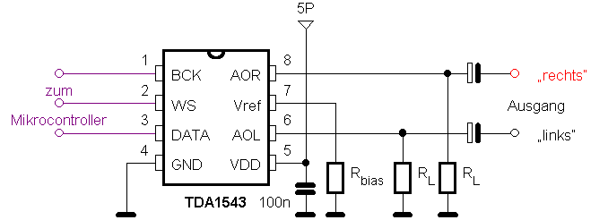
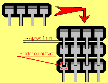
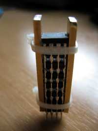
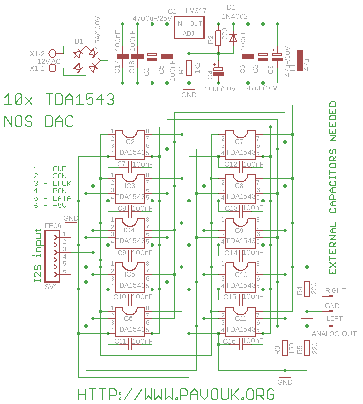
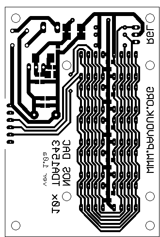
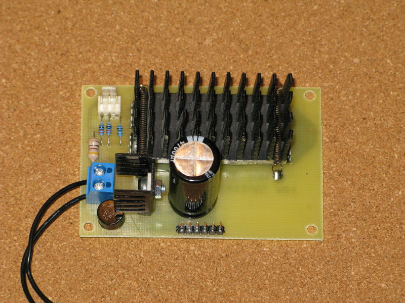
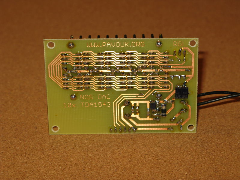
    เหยื่อรายที่ 4 มาแล้วครับ
    เรามาลงชื่อดีกว่าครับ เหยื่อ 11 ท่าน
    1.keang
    2.poh1998
    3.ManiacMaew
    4.jinn
    5.
    6.
    7.
    8.
    9.
    10.
    11.

    Comment


    • #92
      ขอร่วมวงลงชื่อด้วยคนครับ

      Comment


      • #93
        เหยื่อรายที่ 5 มาแล้วครับ
        เรามาลงชื่อดีกว่าครับ เหยื่อ 11 ท่าน
        1.keang
        2.poh1998
        3.ManiacMaew
        4.jinn
        5.Hanzo
        6.
        7.
        8.
        9.
        10.
        11.

        Comment


        • #94
          ผมขอด้วยคนครับ

          Comment


          • #95
            Originally posted by MONOLAB
            XO 12Mhz ท่าน keang ลองไปดูที่
            บ้านหม้อพลาซ่าครับ ขึ้นบันไดตรงที่ขาย C แปลกๆครับ
            เดินไปเลี้ยวขวาอ้อมมาด้านหลัง จะเห็นมีร้านป้าแก่ๆหน้าร้านจะมี
            ซิ้งตัวเล็กๆขายอยู่หลายๆแบบครับในตู้กระจกจะมี XO 12Mhz ขายอยู่ครับ
            ตัวล่ะ 30 บาท
            ผมไม่ทราบว่าเป็น TTL หรือ CMOS นะครับ
            ถ้า CMOS ก็ 5V TTL ก็ป้อน 3.3V
            ร้านที่ผมแนะนำให้ตอนแรกนั้นมันเป็น TCXO นะครับตัวล่ะ 30 บาท
            วันนี้ไปเดินบ้านหม้อ เดินหาร้านที่คุณmonolabแนะนำ วน3รอบได้มั้งถึงเจอ

            สรุป ผมได้TCXOแบบFull Size เป็นของไทหวัน ความถี่12.000MHzแล้ว
            ที่ดีใจสุดๆ คือ ร้านเค้ามีTCXOความถี่6.000MHzด้วย (โปรเจคสำหรับTAS1020Bไม่เป็นหมันละ)
            ราคาหน้าร้าน ตัวละ35บาท ซื้อหลายตัวเหลือ30บาท


            สเปคคร่าวๆของ TCXO ที่ซื้อมา > pdf datasheet
            Supply Voltage = 5Vdc, 20mA
            Frequency Stability = 25ppm / Aging = 5ppm/year Max
            Rise and Fall Time(Tr,Tf) 10% to 90% of Waveform W/Hcmos Load = 5ns Max
            Output Voltage Logic High = 4.5V min / Output Voltage Logic Low = 0.5Vdc max
            Output Signal = 10TTL Load or 50pF HCMOS Load
            Last edited by keang; 7 Oct 2011, 08:18:20.

            Comment


            • #96
              Originally posted by keang View Post
              วันนี้ไปเดินบ้านหม้อ เดินหาร้านที่คุณmonolabแนะนำ วน3รอบได้มั้งถึงเจอ

              สรุป ผมได้TCXOแบบFull Size เป็นของไทหวัน ความถี่12.000MHzแล้ว
              ที่ดีใจสุดๆ คือ ร้านเค้ามีTCXOความถี่6.000MHzด้วย (โปรเจคสำหรับTAS1020Bไม่เป็นหมันละ)
              ราคาหน้าร้าน ตัวละ35บาท ซื้อหลายตัวเหลือ30บาท

              TCXOที่ได้มาเป็นแบบใช้ไฟเลี้ยง 5Vdc, 20mA, 25ppm (5ppm/year Max), 10TTL Load or 50pF HCMOS Load
              ร้านมันอยู่ชั้น2ใช่มั้ยครับ? เดี๊ยวได้ไปหามาเตรียมไว้บ้าง

              Comment


              • #97
                เหยื่อรายที่ 6 มาแล้วครับ
                เรามาลงชื่อดีกว่าครับ เหยื่อ 11 ท่าน
                1.keang
                2.poh1998
                3.ManiacMaew
                4.jinn
                5.Hanzo
                6.Tanasothon
                7.
                8.
                9.
                10.
                11.

                Comment


                • #98
                  ^
                  ผมถูกหลอกง่ายเอาไปเป็นเหยื่อด้วยคน.....
                  ความสามารถจะถึงมั๊ยนี่....555+

                  เอาที่ 11 นะ เสือตัวที่11

                  Comment


                  • #99
                    เหยื่อรายที่ 7 มาแล้วครับ
                    เรามาลงชื่อดีกว่าครับ เหยื่อ 11 ท่าน
                    1.keang
                    2.poh1998
                    3.ManiacMaew
                    4.jinn
                    5.Hanzo
                    6.Tanasothon
                    7.
                    8.
                    9.
                    10.
                    11.tiger X-fi

                    Comment


                    • Originally posted by dracoV
                      มีเทคนิดการขนาน IC อย่างไร เอามาแนะนำกัน ได้เป็นแนวทางครับ
                      - ผมชอบวิธีต่อซ้อนเป็นคอนโด เพราะ เส้นทางสัญญาณสั้นสุด และไม่มีปัญหาเรื่องการดีเลย์ของสัญญาณที่ส่งไปให้ชิบDACแต่ละตัว
                      แต่วิธีนี้จะมีปัญหาเรื่องความร้อน ฉะนั้นต้องหาวิธีช่วยระบายความร้อนดีๆด้วย

                      - TDA1543 ขา7(Vref) Rbias
                      Rbias ค่าความต้านทานจะเปลี่ยนตามโหลด(Voutput)และจำนวนการขนานชิบDAC


                      ------------------------------------------------------------


                      ตัวอย่างวงจรและวิธีต่อขนานชิบDAC ที่มีการเผยแพร่ในเนท


                      เครดิต > Doede Douma

                      Some Details on how to build the TDA1543 DAC-Tower

                      I had several questions on how the DAC tower was made, so try to give some idea here....


                      Actually what I did was start with one DAC-chip, take the next one, put it on top of the first one so pin 1 is touching pin 1, 2->2 ,3_>3, etc. So in fact the DACs are fully parallel !! Make sure to leave approximately 1 mm in between the chips top en bottom, allowing for air to flow between the chips. Continue this procedure till you reach the desired TOWER !!


                      To complete the tower, I have mounted to copper strips at the sides for heat dissipating and transport. Extra to this you can glue small cooling elements at the side with special heat conducting glue (from your Electronics shop...) The tower gets really cooking hot, so I also have built in small mini FAN. This fan normally operates at 12 volt, but then it is blows like hell and is very load, bit overkill.... What I did is putting a resistor in series, till the Voltage over the fan was aprox 6 Volt. Now it runs very smooth and silent and still moves sufficient air to cool the tower. Of course I mounted the fan in such a way, it blows directly at the tower, from 7 cm distance or so.....

                      Hope this clear things up a bit !!!!


                      ------------------------------------------------------------


                      TDA1543 x4 parallel


                      ------------------------------------------------------------


                      เครดิต > pavouk

                      TDA1543 x10 DAC Module
                      pcb > eagle 5 format


                      ------------------------------------------------------------


                      เครดิต > Lesha's DAC

                      TDA1541 x2 Lesha's DAC

                      TDA1541 x2 Parallel

                      DAC part uses two TDA1541s in parallel and passive I/V conversion with 30 Ohm resistors and 0.1uF polystyrene caps per chip. This gives 60mV amplitude of output signal. The resistors are common for both chips (thus they are 15 Ohm), the caps are separate for each chip. Connecting pins 16 of TDA1541s together synchronizes their active divider clock generators resulting in a much sharper sound image. The active divider bypass capacitance is chosen higher than the value from the datasheet for better dynamics and bass. Further increasing the capacitance is limited by the capacitor size, it becomes hard to fit rather good quality caps close to the TDA1541s.

                      IMPORTANT NOTE: Though myself and other people had no problem with pin 16 connection I had one report of severe distortion caused by this. If you have a distortion problems with the DAC please try to disconnect pins 16.

                      The regulators do not have global negative feedback. They are designed to provide perfect stability and <2mV noise+hum for digital +/-5V supplies and <1mV noise and hum for analog -15V supply in 100Hz to tens of MHz band. The output impedance within the band is below 1 Ohm for +/-5V supplies and 0.6 Ohm for -15V supply. The digital +/-5V supply regulators are usual Zener + follower curcuit, the -15V uses a red GaAsP LED as voltage reference (Zeners are rather noisy), its voltage is amplified (in inverse polarity) by Q4 and supplied to the emitter follower. The -5V supply is decoupled from -15V supply by C46 and R6. A separate supply can be used for -5V but it seems to give no advantage. +9V and -21V are the minimal input voltages required for normal operation, these voltages can be significantly higher (up to say +15V and -30V). The LED should not be used as an indicator. It is rather dim because it is used at low current.

                      Parts:
                      Attention should be payed to the I/V resistors (R1, R2) quality. These should be high grade metal film or noninductive wirewound (different sound) type. You may need to try different types to attain the sound you like most.

                      The active divider bypass caps (C5..C18, C23..C36) and the nonpolar caps in the power supply (C41, C42, C45, C49) should be 63V polyester or polypropylene. The -15V regulator output bypass cap (C47) should be paper in oil or polypropylene. The output filter caps (C37..C40) and -15V power supply bypass caps (C4, C22) should be polystyrene or mica. The +/-5V supply bypass caps (C2, C3, C20, C21) and active divider timing caps (C1, C19) should be NPO/COG ceramic or mica or polystyrene.

                      The 2SC1061 and 2SB1015 transistors can be replaced with TIP31 and TIP32 respectively. They are dissipating rather low power and can be used without heatsinks. Smaller transistors in TO126 or even TO92MOD cases can be used instead but they may require heatsinks.
                      R10 may need adjustment depending on LED type, increase it to reduce the output voltage. A yellow or green LED can be used as well but they require higher R10. Try 110 Ohm for R10 first then measure the voltage across R10 and set R10 to the voltage measured/0.01A (that is for 1.1V across R10 it should be 110 Ohm).


                      อันนี้ของแถม เพราะไม่เกี่ยวกับเรื่องขนานชิบdac

                      CS8412 Digital Receiver

                      Digital part contains CS8412 receiver in its textbook configuration and the indicator circuit. The two-color LED indicates both power on (red) and valid data (green). CS8412 is shielded with copper foil and the shield is connected to analog ground pin (pin 21). If you build your own digital part or use the DAC as a part of CD player the output signal should be in standard IIS format. If two separate LEDs are used the indication circuit can be simplified: R6, R7 and Q2 should be removed and the upper terminal of R8 should be connected directly to +5V. This way the red (power) LED will be on as long as the power is supplied.

                      CS8412 Digital Receiver with async reclocking

                      Digital part with async reclocking. This is preliminary and displays the current state of my DAC. The basics of async reclocking are described in an article by Ryohei Kusunoki. Here U4, U5, U7 form an asynchronous clock source with complementary outputs, U6 forms a master-slave D-flop which performs reclocking and is resistant to latching at the input signal transitions (the slave D-flop latches half clock period after the master one so the master one comes into a defined state at that time). The schematic is very preliminary, definitely the clock source must be improved.
                      Last edited by keang; 7 Oct 2011, 10:05:04.

                      Comment


                      • ขอเป็นเหยื่อด้วยคน ได้หรือปล่าวครับ

                        Comment


                        • Originally posted by sornuk View Post
                          ขอเป็นเหยื่อด้วยคน ได้หรือปล่าวครับ
                          ได้แน่นอนอยู่แล้วครับ
                          เหยื่อรายที่ 8 มาแล้วครับ
                          เรามาลงชื่อดีกว่าครับ เหยื่อ 11 ท่าน
                          1.keang
                          2.poh1998
                          3.ManiacMaew
                          4.jinn
                          5.Hanzo
                          6.Tanasothon
                          7.sornuk
                          8.
                          9.
                          10.
                          11.tiger X-fi

                          Comment


                          • กระทู้ต้นเหตุ > [Review] Audio-GD NFB-12 หน้า2 #29

                            Originally posted by keang
                            มีความคิดอยากลองเปิดฝาเครื่องNFB-12เล่นไรหนุกๆป่าวครับ
                            ไม่ต้องทำไรมากด้วย แค่ใช้นิ้วปลดไรบางอย่างออก แล้วฟังเสียงเทียบก่อนกับหลังปลดตัวนั้นออก
                            Originally posted by keang
                            เปิดฝาบน จะเห็นอินพุทชุดOPTIC อินพุทชุดนี้จะเป็นแบบโมดูล ใช้คอนเนคเตอร์เสียบที่PCBหลัก
                            ลองง่ายๆ ถอดคอนเนคเตอร์ของชุดOPTICออก แล้วฟังเสียงเทียบกันครับ


                            มารายงานผลครับแต่จริงๆก็คือ วันนี้ยุ่งทั้งวันก็เลยได้ลองแป๊ปเดี๋ยวนะครับ ความเห็นส่วนตัว ผมว่าเสียงต่างกันครับแต่ดีกว่าหรือเปล่าไม่แน่ใจครับ เพราะไม่มีเวลามาลองตั้งใจฟังครับ
                            ในที่สุดก็ได้ลองซนกับ GD ตามที่พี่โก้แนะนำครับ

                            ผลที่ได้คือมันโปร่งกว่าเดิม สะอาดกว่าเดิม และเสียงเป็นรูปเป็นร่างมากกว่าเดิม
                            แถมยังถ่ายโอนไปมาซ้ายขวาได้เคลียกว่าเดิมด้วยครับ
                            ว่าแต่ทำไมมันส่งผลได้เยอะพอสมควรเลยครับ แค่ดึงคอนเนคเตอร์ออกเองครับ

                            ------------------------------------------------------------------------------


                            ก่อนหน้านี้ เคยยุให้เพื่อนในนี้2คนลองสนุกกับพอร์ทOpticalของเครื่องDAC

                            ทั้ง2คนไม่ได้ใช้งานพอร์ทออปติค ผมเลยให้เค้าลองถอดPCBชุดพอร์ทออปติคออกแล้วลองฟังเสียงเปรียบเทียบ
                            ซึ่งทั้ง2คนก็บอกผลออกมาในแนวเดียวกันว่า มีผลต่าง

                            เค้าก็เลยPMมาถาม เพราะสงสัยว่า เหตุใดมันถึงให้ความแตกต่างได้ ผมก็ตอบกลับไปแบบข้างล่างนี้
                            ผิดถูกไม่รู้น่ะ มั่วไว้ก่อน คนอ่านใช้วิจารณญาณในการอ่านด้วยละครับ


                            ------------------------------------------------------------------------------


                            คิดง่ายๆแบบนี้ครับ

                            พอร์ทออปติคที่ทำหน้าที่เป็นตัวส่ง
                            - พอร์ทออปติค ภายในมันมีหลอดไฟ(เราจะเห็นเป็นสีแดง) ซึ่งหลอดไฟก็ใช้ไฟเลี้ยงด้วย
                            - พอร์ทออปติค ปรกติพอเปิดเครื่องมันก็ทำงานทันที (ถ้าเป็นเครื่องแบรนด์ตัวท็อปผู้ผลิตถึงจะใส่ออปชั่นให้เลือกปิดเปิดได้)


                            ส่วนของระบบภาคจ่ายไฟ
                            หลอดไฟภายในตัวพอร์ทออปติคใช้ไฟเลี้ยง5โวลท์ ซึ่งจะไปตรงกับแรงดันไฟชุดดิจิตอล ที่ใช้จ่ายไฟเลี้ยงไอซีดิจิตอลในเครื่องทั้งหมด
                            ผู้ผลิตเครื่องส่วนใหญ่ จะไปแชร์ไฟจากชุดดิจิตอลมาจ่ายให้หลอดไฟตัวนี้ด้วย
                            ( ซึ่งเครื่องตลาดระดับล่างถึงระดับบน 98%ไม่มีการแยกชุดจ่ายไฟให้LEDของพอร์ทออปติค แม้แต่ตัวไฮเอนด์ท็อปหลายยี่ห้อยังไม่แยกให้เลย )

                            พอร์ทออปติค เวลาทำการส่งข้อมูล หลอดไฟจะกระพริบ พอมันกระพริบก็ส่งผลให้ระดับแรงดันไฟเลี้ยงชุด5โวลท์ไม่นิ่ง
                            พูดง่ายๆก็คือ ทำให้ไฟเลี้ยงชุด5โวลท์มีการกระเพื่อมตามจังหวะการกระพริบของหลอดไฟ

                            ผลต่อมาก็คือ การกระเพื่อมตามการกระพริบของหลอดไฟ จะเปรียบเสมือนเป็นสัญญาณรบกวนย้อนกลับไปหาวงจรภาคจ่ายไฟด้วย

                            ตัวอย่าง : ความถี่ของสัญญาณรบกวนก็จะเท่ากับจำนวนการกระพริบต่อ1วินาที กระพริบ120ครั้ง/วินาที=ความถี่120เฮิร์ช/วินาที

                            ถึงตรงนี้ เราจะรู้ผลกระทบได้2เรื่องแล้ว
                            1. แรงดันไฟชุด5โวลท์ไม่นิ่ง เพราะ มีการกระเพื่อนขึ้นลงตามจังหวะการกระพริบของหลอดไฟ
                            2. แรงดันไฟชุด5โวลท์มีสัญญาณรบกวนเกิดขึ้น เพราะ การกระพริบของหลอดไฟ


                            ส่วนของระบบสัญญาณดิจิตอลที่ส่งไปที่พอร์ทออปติค
                            ในเครื่องDACจะรับสัญญาณดิจิตอลS/PDIFจากชุดอินพุท แล้วส่งไปที่ชิบDigital Receiver
                            เช่น CS8412, 8414, 8416 / WM8804, WM8805 / DIR9001 / TAS1020B

                            สัญญาณดิจิตอลเอ้าท์พุทของชิบDigital Receiver ก็จะปล่อยออกมาหลายอย่าง
                            - S/PDIF (Digital Out 1เส้น)
                            - I2S (3เส้น)
                            สัญญาณพวกนี้จะส่งต่อให้ชิบDACอีกที

                            พอร์ทออปติคจะไปแชร์ดึงสัญญาณดิจิตอลS/PDIFจากขาDigital OutของชิบDigital Receiver

                            เท่ากับว่า ในขณะที่เครื่องDACทำงานนั้น สัญญาณชุดS/PDIFมีการแบ่งออกเป็น2ทาง (เหมือนพ่วงสายไฟ หรือ สายY)
                            - ส่งไปชิบDAC
                            - ส่งไปพอร์ทออปติค

                            ขี้เกียจอธิบายยาวน่ะ เอาแบบคร่าวๆแล้วกัน เพราะผลมันแบบเดียวกับที่เกิดกับระบบไฟเลี้ยงข้างบน
                            ขณะที่หลอดไฟของพอร์ทออปติคกระพริบติดๆดับๆ ก็จะมีสัญญาณรบกวนย้อนกลับไปหาชิบDigital ReceiverและชิบDACด้วย


                            ------------------------------------------------------


                            พอร์ทออปติคที่ทำหน้าที่เป็นตัวรับ
                            - พอร์ทออปติคด้านตัวรับ ใช้ไฟเลี้ยง5โวลท์ (ส่วนใหญ่ใช้ไฟร่วมกับชุดไฟเลี้ยง5โวลท์ของชุดไอซีดิจิตอล)
                            - พอร์ทออปติคด้านตัวรับ เราจะไม่เห็นแสงไฟจากตัวมัน
                            - พอร์ทออปติคด้านตัวรับ ในขณะที่มันทำงาน มันจะรอรับแสงไฟจากด้านตัวส่ง


                            ส่วนของระบบภาคจ่ายไฟ
                            ในเครื่องDACที่มีพอร์ทอินพุทแบบออปติคกับโคแอค จะมีสวิทช์เลือกอินพุทที่หน้าเครื่องว่าจะรับอินพุททางช่องทางไหน
                            ซึ่งสวิทช์ตัวนี้ จะเป็นสวิทช์ที่ทำหน้าที่เพียงเลือกเส้นทางสัญญาณเท่านั้น ไม่ได้ทำหน้าครอบคลุมไปถึงการตัดต่อปิดเปิดไฟเลี้ยงพอร์ทออปติคด้วย
                            ฉะนั้น เมื่อคุณเปิดเครื่องDAC จะมีไฟเลี้ยง5โวลท์ไปจ่ายให้พอร์ทออปติคตลอดเวลา
                            พอร์ทออปติคภายในจะประกอบไปด้วยอะหลั่ยหลายตัว เช่น โฟโต้ไดโอด(ตัวรับแสง), ตัวเก็บประจุ, บางวงจรอาจจะใส่ขดลวด(L)หรือตัวต้านทาน(R)ที่ขาไฟเลี้ยงด้วย

                            ดังนั้น วงจรในส่วนของพอร์ทออปติค จะมีค่าC,ค่าR,ค่าLอยู่ภายในตัวเองด้วย ซึ่งผลจากค่าC,R,Lนี้ จะเกิดผลเป็นค่าอิมพิแดนซ์ของตัวมันเอง
                            ค่าอิมพิแดนซ์ของวงจรพอร์ทออปติค จะมีผลเชื่อมโยงไปถึงค่าอิมพิแดนซ์ภาคจ่ายไฟด้วย เพราะค่าอิมพิแดนซ์ของภาคจ่ายไฟจะเปลี่ยนแปลงตามไปด้วย


                            ส่วนของระบบสัญญาณดิจิตอลที่รับเข้าทางพอร์ทออปติค
                            ในขณะที่ตัวรับของพอร์ทออปติครับข้อมูลเข้ามา ตัวรับแสงภายในก็จะเกิดลักษณะแบบเดียวกับพอร์ทออปตัคด้านตัวส่ง คือ คล้ายๆหลอดไฟติดๆดับ
                            ( ไม่รู้จะอธิบายเป็นตัวอักษรยังงัย ประมาณว่ามันดีเทคว่ามีแสงหรือไม่มีแสงส่องมาหาตัวมัน )

                            ซึ่งจังหวะกระพริบติดดับนี้ จะเกิดผลเอฟเฟคแบบเดียวกับที่เกิดกับด้านตัวส่ง เพราะมันไปมีผลกับไฟเลี้ยง5โวลท์ของชิบไอซีดิจิตอลด้วย


                            ไม่ไหวละ คนอธิบายเอง โม้ไปก็เริ่มมึนเองแล้ว
                            Last edited by keang; 7 Oct 2011, 14:01:20.

                            Comment


                            • เนื่องจากไม่มีคนสนใจลงชื่อ ขอปิดที่ 8 ท่านก็แล้วกันครับ เก็บไอซีไว้โครงการต่อไป
                              1.keang
                              2.poh1998
                              3.ManiacMaew
                              4.jinn
                              5.Hanzo
                              6.Tanasothon
                              7.sornuk
                              8.-
                              9.-
                              10.-
                              11.tiger X-fi

                              Comment


                              • ไม่ทัน 5555 ไม่เป็นไรไม่มีเวลาอยู่ดี จะคอยรอชมและกันครับ **ปูเสื่อแถวหน้า

                                Comment

                                Working...
                                X