 Tweet
Tweet
โป๋มาคราวนี้เป็นหนุ่มเลย พัฒนาแบบก้าวกระโดด ต่อยอดชิ้นงานเก่าได้น่าสนใจมาก
-
-
> Modding the Melos SHA-1 Headphone Amplifier
The Melos high voltage power supply consists of some solid state diodes and a p filter formed by two capacitors and a resistor. Now, I have no qualm with solid state diodes (I often use tube rectifiers, but this is primarily for the slow startup characteristics, not because I think they sound better ? they don?t). However, there are diodes, and then there are diodes. The Melos uses, so far as I can tell, some off the shelf cheapies that can withstand the voltage. The problem with this is that bad diodes impart switching noise into the power supply that does not sound good.
The pi filter consists of a 470u cap, a 150R resistor, and a 100u cap. As can be seen, this arrangement results in both high ripple (over 9mV), as well as ripple containing all sorts of high frequency harmonics.

The usual solution to this sort of thing is to add a choke. However, while adding a small choke reduces the ripple to a reasonable level, due to the capacitor arrangement, adding a choke here does not really do much to solve the sharp peaks.

Moreover, also due in large part to the backwards arrangement of the caps (typically you want the caps to increase in a high voltage supply), the addition of the choke causes ringing.

After futzing around with the original board, the solution here was to just tear the whole mess out and redo it. To this end, I first used super low switching noise avalanche diodes. These have about 25db less switching noise than standard rectifiers due to what are essentially built-in snubber caps. Additionally, I reduced the cap size (I find large caps in tube power supplies tend to make things muddy) and added a choke. I also added an extra filtering stage to make up for the smaller caps. While this is still not perfect, it is way better ? the ripple is smooth and small ? more than an order of magnitude smaller than it was before.

... and it doesn't ring.

 Last edited by keang; 24 Apr 2014, 15:12:13.
Comment
-
> hifidiy : 47Labs Model 4706 Gaincard
> diyAudio : internals 47 labs 4717 integrated
> diy Audio Village : อีกสักครั้งกับ Shigaclone LM1875
4717 Shigaraki


ปริ๊นตัวจริง ดีไซน์เอนกประสงค์จริงๆ เนื้อทองแดงเป็นจุดพักhardwire-point2pointLast edited by keang; 24 Apr 2014, 20:13:10.Comment
-
เก็บเล็กผสมน้อย
> Power Supply Basics
> Op-Amps - An Introduction
> Hi-Fi Amplifiers for Beginners
----------------------------------------------
Musical Fidelity A1
- original circuit

- Preamp replacement
I decided to use the venerable NE5532 for the preamp. I know that it is an old device, but even today you have to spend a lot of money to improve on it. The biggest advantage is the excellent drive capability, meaning that with a non-inverting configuration, you can have very low-value components in the feedback path, minimising Johnson noise - remember, I was pretty paranoid about this issue at the time.
You can try different op-amps in this circuit, but if you do, I'd recommend that you increase the value of R3 and R4 to reduce the loading on the op-amp, as many of the popular alternatives generate more distortion into loads less than about 2k?. You could simply increase them by a factor of 10 (to 6k8 and 2k2), but I'd recommend 3k and 1K. Good quality but affordable alternatives to the NE5532 include the OPA2604 and the OPA2134. I have tried the latter (with 3K and 1K gain setting resistors), and it worked fine... If trying anything more exotic, do take care with layout and decoupling, as parasitc oscillations are a very real possibility with some of the high-speed options.

The first part of the circuit is an ultrasonic filter. Note that this is simply to avoid noise in the MHz range upsetting the op-amp*, and is not meant to be a bandwidth-setting component. The cut-off frequency varies with source impedance: -3dB @ 340kHz with 0? source impedance, and -3dB @ 190kHz with 1k source impedance. The amplifier bandwidth is set later by R4 and C5 on the main PCB.
The volume control is a good-quality 10k log pot - deliberately low in value to minimise Johnson noise. Modern kit should be quite happy to drive this sort of load, although some exotic valve gear might not like it - in which case feel free to try a 50k instead... This pot is AC-coupled to the op-amp by a non-electrolytic capacitor. As above, the exact -3dB point is variable this time the position of the volume control will influence it. However, it is low enough not to be a problem and the LF cut-off is properly defined by C6 and C7 in the power amplifier.
- Headphone amplifier
This is based around an OPA2134 with a class B buffer formed by bipolar transistors. For most headphones of high to medium impedance, a single NE5532 normally has sufficient drive capability. However, adding the transistor buffer opens up the opamp choice by removing the need for good drive capability. The OPA2134 has a FET input stage, which means the DC offset of the stage is reduced to a few millivolts - this has the very welcome advantage of being able to DC-couple the output thus losing the large electrolytic capacitors that would otherwise be required.

The buffer is included in the feedback loop and is very simple. While there are plenty of ways to improve it, check out on Doug Self's website for reasons why I didn't. That said, One refinement is the addition of the resistor from the opamp output to the buffer output - this enables the opamp to source current when the transistors aren't conducting. This is a very simple form of 'feed-forward' compensation - basically for very small output voltages (or high impedances) the opamp drives the load directly and avoids any cross-over distortion from the class-B buffer.
----------------------------------------------
> A4 Power Amplifier (LM4780)
Op-amp power supply
The OPA2134 is powered from split 15 volt supplies. The unregulated supplies to the amplifier modules are around ?36V, which is on the limit for 7x15 regulators. So I chose a simple shunt power supply using two 12mA current sources and a pair of Zener diodes. The noise generated by the Zeners is filtered by a low-pass filter formed by a 15 ohm resistor and 47uF capacitor, turning over at around 200Hz. This frequency is comfortably low enough to ensure that the op-amps PSRR is sufficiently high to provide good ripple rejection. Finally, a low-ESR 1uF capacitor is connected between the power pins of the op-amp.
This arrangement was arrived at after some experimentation - I found that using standard quality capacitors were best for the 47uF devices, and the 1uF between the supply pins, directly mounted at the IC, was best on its own. Additional ceramic or polyester capacitors didn't provide any additional benefit, either subjectively, or measured at the output or the IC supply pins.

While it looks simple, this power supply is well-suited to this application. The current sources provide excellent isolation from the broadband noise and ripple on the unregulated supply rails. While the Zener diodes might not be the last word in DC precision, they are far better than required here.Last edited by keang; 24 Apr 2014, 22:00:16.Comment
-
กำลังไล่อ่านโพสต์คุณkeang (ยังไม่จบ1โพสต์เลย ฮาๆ )
ก็มาสะดุดตรงนี้

ช่วงปรีแอมป์ของMusical Fidelity A1 ที่วงไว้ตามรูป
หรือมันจะเป็นเคล็ดลับของเขาComment
-
เรื่องเกนขยาย เรื่องเอาวอลลุ่มเป็นฟีคแบค ... ของแบบนี้ต้องลองครับ จะได้รู้ลักษณะผลที่ได้จากของจริง
ร้านขายชุดคิทบ้านเรา เอาวงจรปรีของA1ไปทำขายด้วยแหะ
> Pre Amp Kit - Finish Musical A1

 Last edited by keang; 29 Apr 2014, 23:40:08.
Comment
-
> Basic Buffers
One recurring question often seen is how to add a buffer to a circuit to prevent loading and loss of definition of the guitar sound. Buffers present a high impedance to the guitar pickup and have a low impedance output drive with a gain close to unity (unity gain = 1). This is an excellent addition in front of a vintage wah-wah or other circuit that can rob the signal of high frequency response. Buffers are simple, easy and cheap to construct. (Note: Any of these buffers could also be used on the output of an effect circuit.)
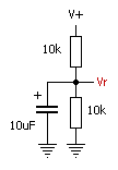
Before we see the circuits let us look at a circuit fragment that may be required for some of the buffer variations. As shown to the left, the resistor/capacitor network provides a reference voltage that may be used to bias the transistor or opamp into the best operating range. The point marked "Vr" is connected to the point also notated as "Vr" on the buffer schematic. If there is a reference voltage already established in a circuit to which you are planning to add a buffered input, the existing Vr can be tapped and used for the buffer's reference.

Probably the easiest buffer is the basic jfet common drain amplifier. The input impedance is determined by the value of R1 and is 1M as shown in this example. The value of R2 is not too critical and may be any value from 3.3k to 10k without much change in the sound. I prefer to use lower values since this allows more drive on the negative portion of the audio cycle where the only pull-down is the source resistor. This configuration has the least number of parts but is limited in that if the input voltage exceeds the gate-source forward voltage plus the bias voltage at the source, the signal will be clipped. This configuration is not normally useful with bipolar or mosfet transistors, which require a positive bias voltage (for N-type devices). Input impedance is approximately the value of R1. The output impedance will depend on the jfet but is on the order of a few hundred ohms.

The basic jfet buffer shown in the last paragraph may be improved upon by connecting the gate resistor to a bias voltage instead of to ground. This allows the gate voltage to set the bias at the source to a higher vlaue which increases the headroom and allows a large signal input before clipping. The Vr point on this circuit connects to a bias voltage source as shown in the first paragraph. Input impedance is again approximately the value of R1. It could easily be increased to 10M or more for a cleaner sound with high impedance signal sources such as high-output humbuckers or piezo sensors with only a slight incerase in the thermal noise contributed by the higher value of R1.

If you do not have a bias source available for Vr and you want to keep down the parts count, the gate bias can be set by a pair of resistors as shown in this example. The input impedance is the value of R1 paralleled by R3, or 500k ohms in this example, but you could easily increase their values to 2M to maintain the 1M input Z. This is the buffer that I used on the front end of the Dr. Quack Envelope Filter.

If you substitute a mosfet transistor into the circuit of the last example and tweak the source and gate resistor values, it is essentially the AMZ Mosfet Booster in buffer mode. (See how these building blocks are useful?) A 9v zener diode (D1) is used for static protection on the mosfet gate. Mosfets have high capacitances between its electrodes and though there is no Miller Effect to multiply those capacitances, their value can nonetheless be high enough to cause high frequency rolloff depending on the characteristics of the individual mosfet transistors.

A bipolar transistor may also be pressed into service if the input impedance does not have to be as high as that available from jfets. The advantage is that the bipolars usually have a lower output impedance and are generally easier to find. The disadvantage is the lower input impedance available as compared to fets.

An alternate configuration is shown here that uses the voltage bias on the input in the same manner as the second jfet example above. This is the buffer used in the TS-series distortion boxes.
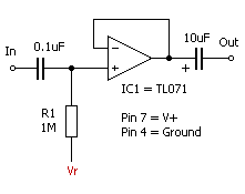
An opamp is an even better buffer amplifier, though many believe they are somewhat colder sounding and more sterile than the transistor versions. The opamp gain is exactly unity and the output impedance is quite low; typically measured in tens of ohms instead of hundreds as with the transistors. It also has the lowest parts count of any of the simple buffers presented here.
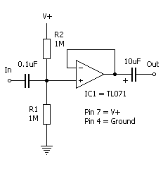
Voltage divider biasing is also possible with the opamp and the input impedance is calculated the same way as with the transistor versions similarly biased.

This opamp buffer inverts the signal, which is useful when used in conjunction with following gain stages that also invert the signal and therefore would make the output non-inverted when compared to the input. This is important if the signal is mixed with other signals from the same source since cancellation could occur otherwise. The gain is unity and is set by R2/R1. The small 5pF capacitor is optional and gradually rolls off the high frequencies above the audible range. The input impedance of this circuit is the value of R1.
Miscellaneous :
Selection of the jfet or bipolar type is not critical, almost any transistor will work fine without problems. The gain of the transistor versions is slightly less than 1, probably 0.9 to 0.96. Transistors with higher hfe will be slightly closer to unity gain.
The transistor circuits have very poor power supply noise rejection. Battery power works well with them but if used with an AC adapter, it must be well filtered and hum-free or the noise will be combined with the signal.
For the jfet or mosfet circuits that use a single resistor on the gate for bias, you can increase the value of R1 to provide a higher input impedance. I typically use jfets on inputs and bipolars for output buffers where their better drive characteristics are needed.
While this article just scratches the surface of buffer amplifiers, it presents enough basic circuits to handle 99% of effects requirements. Any of the building blocks above may be dropped into a circuit exactly as presented.
--------------------------------------------------
> Current amplifier and buffers
Buffer amplifier
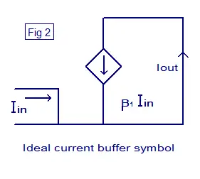
Buffer amplifier is a circuit which transforms electrical impedance from one circuit to another. The main purpose of a buffer is to prevent the loading of a preceding circuit by the succeeding one. For example, a sensor may have the capability to produce a voltage or current corresponding to a particular physical quantity it sense but it may not have the power to drive circuitry it is connected to. In such situations a buffer can be used. A buffer when connected between the sensor and the succeeding circuitry easily drives the circuitry in terms of current or voltage according to the sensor output.Buffers are classified into voltage buffers and current buffers. The symbols of ideal voltage buffer and current buffer are shown in Fig 1 and Fig 2 respectively.
- Fig 1 : Ideal voltage buffer symbol

- Fig 2 : Ideal current buffer symbol
>> Voltage buffer <<
A circuit which transfers a voltage from a circuit with high output impedance to a circuit with low input impedance is call a voltage buffer. The voltage buffer connected between these two circuit prevents the low input impedance circuit ( second one) from loading the first one. Infinite input impedance, zero output impedance, absolute linearity, high speed etc are the features on an ideal voltage buffer.
If the voltage is transferred from the first circuit to the second circuit without any change in amplitude, then such a circuit is called unity gain voltage buffer or voltage follower. The output voltage just tracks or follows the input voltage. The voltage gain of the voltage follower is unity (Av = 1). Even though there is no voltage gain, there will be a sufficient amount of gain in current. So when a voltage follower is connected between two circuit, it will transfer the voltage from first one to second one without any change in amplitude and drives the second circuit without loading the first circuit.
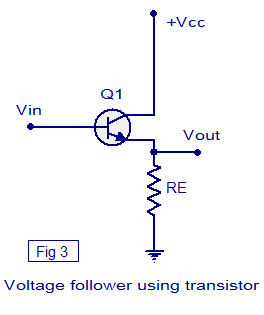
A voltage buffer can be realized using opamp, BJT or MOSFET. Voltage follower using transistor (BJT) is shown in Fig 3. Voltage follower using BJT is also known as emitter follower. +Vcc is the transistor?s collector voltage, Vin is the input voltage, Vout is the output voltage and Re is the transistors emitter resistor.
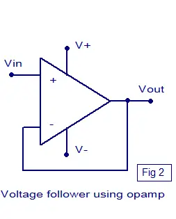
Voltage follower implemented using opamp is shown in Fig 2. This is done by applying full series negative feedback to the opamp ie; by connecting the output pin to the inverting input pin. Here the opamp is configured in non inverting mode (refer Figure 2). So the equation for gain is Av= 1 + (Rf/R1).
Since output and inverting input are shorted ,Rf=0 .
Since there is no R1 to ground, it can be considered as an open circuit and so R1 = ?
There fore (Rf/R1) = (0/?) = 0.
Therefore Voltage gain Av = 1 + (Rf/R1) = 1+0 =1.
>> Current buffer <<
Current buffer is a circuit that is used to transfer current from a low input impedance circuit to a circuit having high input impedance. The current buffer circuit connected in between the two circuits prevents the second circuit from loading the first circuit. The features of an ideal current buffer are infinite input impedance, zero output impedance, high linearity and fast response. A current buffer with unity gain (B=1) is called a unity gain current buffer or current follower. Here the output current just tracks or follows the input current. A current buffer can be realised using transistor (BJT or MOSFET).
Current amplifier circuit
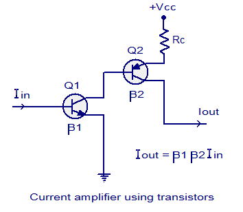
A current amplifier circuit is a circuit which amplifies the input current by a fixed factor and feeds it to the succeeding circuit. A current amplifier is somewhat similar to a voltage buffer but the difference is that an ideal voltage buffer will try to deliver whatever current required by the load while keeping the input and output voltages same, where a current amplifier supplies the succeeding stage with a current that is a fixed multiple of the input current. A current amplifier can be realized using transistors.The schematic of a current amplifier circuit using transistors is shown in the figure below. Two transistors are used in this circuit. ?1 and ?2 are the current gains of transistors Q1 and Q2 respectively. Iin is the input current, Iout is the output current and+Vcc is the transistor T2?s collector voltage The equation for the output current is Iout = ?1 ?2 Iin .
Comment
-
ใครเดินเล่นแล้วเจอ บริดจ์ไดโอดของโมโต ตัวแบบนี้ หน้าตาแบบนี้ อยากลองเสียเงิน เพื่อลองเสียง ก็ลองดูนะ ... อาจจะชอบหรือไม่ชอบก็ได้
ผมชอบเสียงของ MDA990-x แพคเกจแบบดั้งเดิม ใช้กับอินทิเกรทME-3, แอมป์มอสเฟทตัวเล็ก, ปรีหลอด ใส่ทั้งไฟไส้หลอดไฟสูง ... ฟังแล้วเพลิดเพลินได้รมณ์
MDA990กับแบบแพคเกจใหม่ ตรงกลางเป็นอลูมิเนียม จับยึดลงกล่อง,แท่นเครื่อง เป็นการลงกราวน์ไปในตัว เป็นการช่วยเรื่องลดสัญญาณรบกวน
- Motorola MDA980-2 100v 12A รูปแพคเกจแบบดั้งเดิม

- Motorola MDA990-1 50V 30A รูปแพคเกจแบบดั้งเดิม
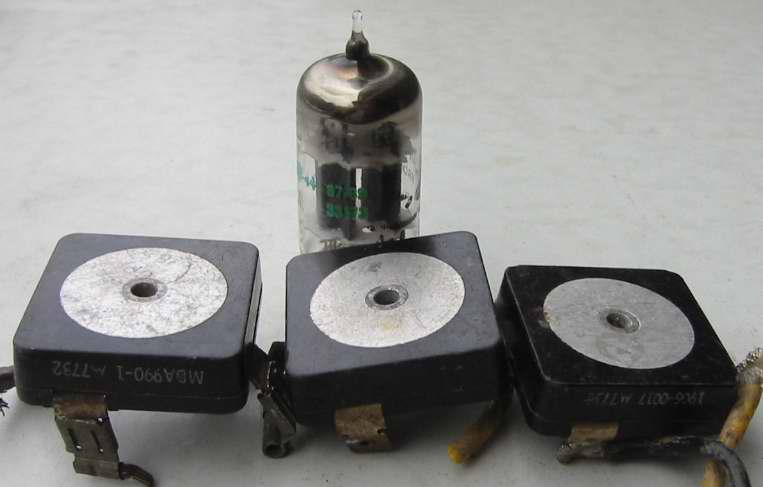
- Motorola MDA980-2 100v 12A รูปแพคเกจแบบใหม่ เริ่มใช้ประมาณปี198xจนถึงปัจจุบัน

MDA980 = 12A , MDA990 = 30A
1 = 50V , 2 = 100V , 3 = 200V , 4 = 300V , 5 = 400V , 6 = 600VComment
-
โปรแกรมช่วยคำนวนค่าอะหลั่ยในวงจรเรคกูเลเตอร์แบบใช้ไอซีสำเร็จรูป
Regulator Design 1.3 > download
- LM317 (LM150 , LM350) voltage regulator
- LM317 (LM150 , LM350) current regulator
- L200 voltage and/or current regulator
- TL431 precision shunt regulator
- TL431 precision shunt regulator (with LM317)
- M5237 3-terminal adjustable regulator
- 78xx series voltage regulator
- 78xx series current regulator
- uA723 precision voltage and/or current regulator
-----------------------------------
Stabilizer heating power lamps
Stable heating power = stable emission cathode, regardless of the supply voltage or aging lamps. Allows you to stabilize the lamp data throughout its life (and not smooth at the standard of care as powering the heater). Also limits the starting heating power (at the cold glow) that extends the life of the lamp.
Input voltage at least 10.5 V at rated voltage network tries. Performance is maintained until 9.6 V which corresponds to 10% trying to network. Home heating power (in cold filament) is equal to half of the nominal value.
 Last edited by keang; 4 May 2014, 11:23:59.
Comment
-
I/V for the DAC s current vihodom
The only drawback of the proposed converter I/V discrete bipolar transistors is:
- A relatively large area that it occupies on the board.
- For maximum performance you need to ensure close to the ideal and complementary transistors VT7 VT9.
It was therefore decided to develop a new inverter I/V which does not have these disadvantages and provide even better quality. The scheme proposed converter I/V with 2nd order lowpass filter with a stable group delay shown in the attachment (with options for DAC curves. 2mya current + (PCM63, PCM1700, TDA1541, TDA1540), +-1mA (AD1856, AD1851, AD1860, AD1861 , AD1862, PCM56, PCM51, PCM61, PCM58, PCM64, PCM1702, PCM1704) and PCM67/69.
Capacitors C1, C2, C3 should be of the highest quality (NP0, foil polypropylene, polystyrene). Resistors R1, R3, R4 carbon (Riken Ohm, Ohmite Little Demon, Ohmite Little Rebel, Allen Bradley, etc) or tantalum or qualitative metalofolgovye, the output T may be used filter requirements for an application of the same parts as described above.
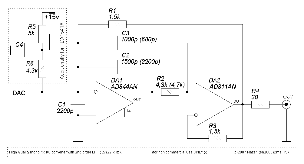
For 2x 1541 or parallel conveyor 750 R1 = R2 = 2.2k C1 = 1500p C2 = 3900p
4x for 1541 R1 = 390 R2 = 1.2k C1 = 3300p C2 = 7500p
30kHz for C2 = C3 = 560pf 560pf

Good luck and good sound!
Literature:
1) M. Hawksford "Current-steering transimpedance amplifiers for high-resolution digital-to-analogue converters", 109th AES Convention, Los Angeles, September 2000
2) E.Barnes "Current feedback amplifiers" Analog dialogue 30-3, 30-4
3) I.Dostal "Operational Amplifiers" Moscow "Mir" 1982r.
4) P. Horowitz, U.Hill "Art circuitry" Moscow "Mir" 1998r.
5) Marcinkevi?ius, Bagdanskis "Speed ??ICs DAC and ADC and measuring their parameters" Moscow 1988r.
6) Documentation of the AD844, AD846, AD811
-------------------------------
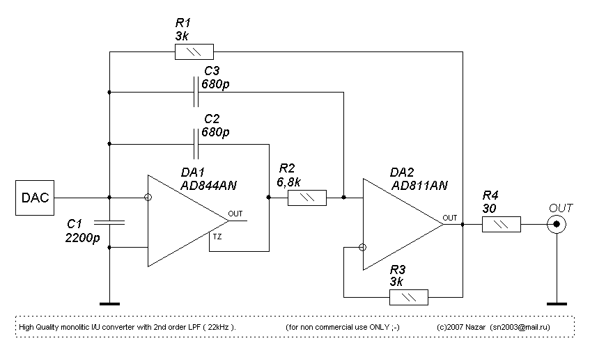
I/V for the DAC s current vihodom 2
Inverter current \ voltage with a frequency-dependent Wasps referred to as "844 5534" was developed neskolkolet ago and has shown good results, but was quickly made ??a small change in the scheme provide a better suppression band LPF detention and to ensure the best outcome subjectively. True, I had not bothered to paint and put this change, but the same answer all the time by e-mail, etc. is already a little tired of the same seen so little time to draw this option, which you can see below for a converter for PCM63 and PCM1702 / PCM1704.
Resistors in a T-filter at the output node and a resistor R1 to be the finest quality, it is desirable metalofolgovye also resistors in a T-filter can be replaced by suitable powerful (for the current 5-10A) ferrite beads.
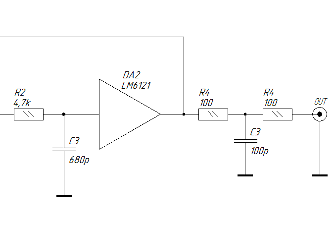
For those who want to get a different sound can experiment with the output buffer, some versions of which are shown below, for example good monolithic buffers type BUF03, LM6121. Or discrete bipolar or FET. Each of the options will only give him a little inherent color. In the case of DU as a buffer to ensure the accuracy of sound is better to use vysokolineynye OS (in the case of ensuring the correct wiring \ lock for their normal operation) type LME49990, LME49710, LT1468, SE5534 (their chains correction) and LM6171. For lovers of the great and persistent stains, you can use certain types of OS specifically for this purpose, for example OP42, OPA604 etc..
In general, experiment to your taste.

-------------------------------
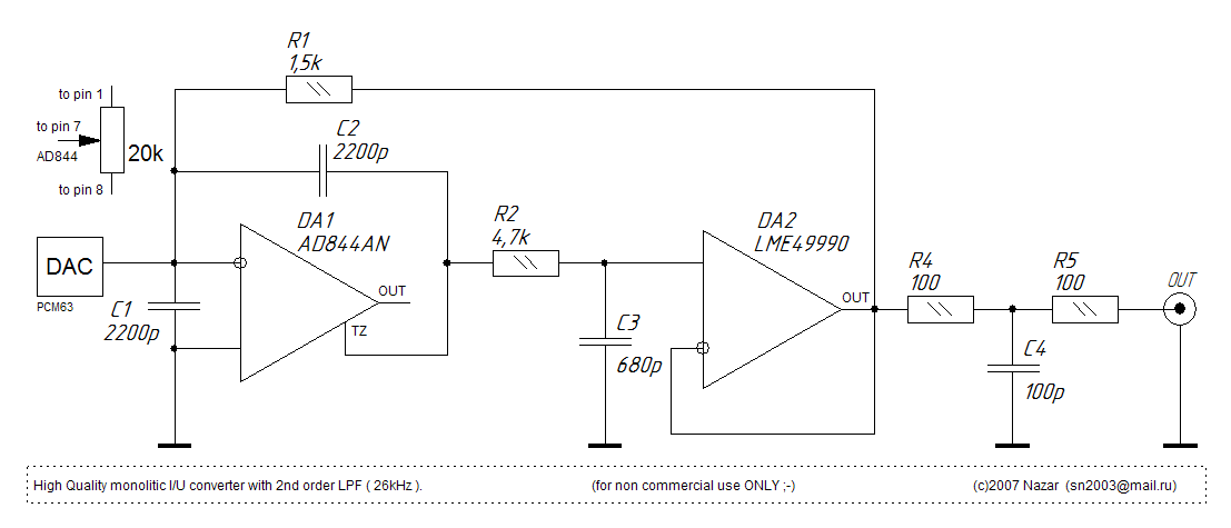
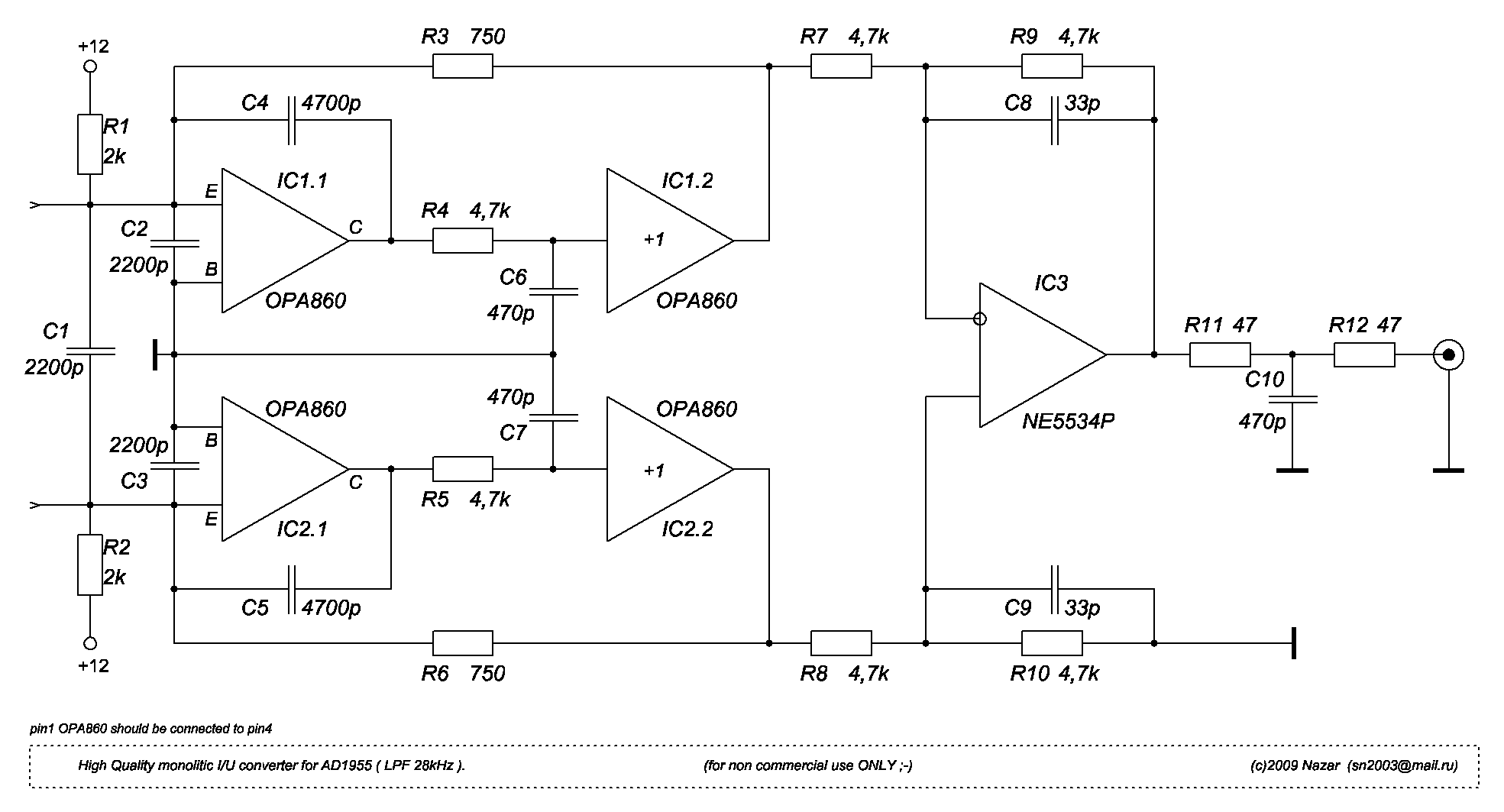
I/V for AD1955
Food OPA860 + -5,5 in op amp differential. need to use the amplifier LME49710, LME49870, LM318, LT1468, LM6171 or any other food to taste + 12c. Resistors desirable MELF, capacitors exclusively NP0.
-------------------------------
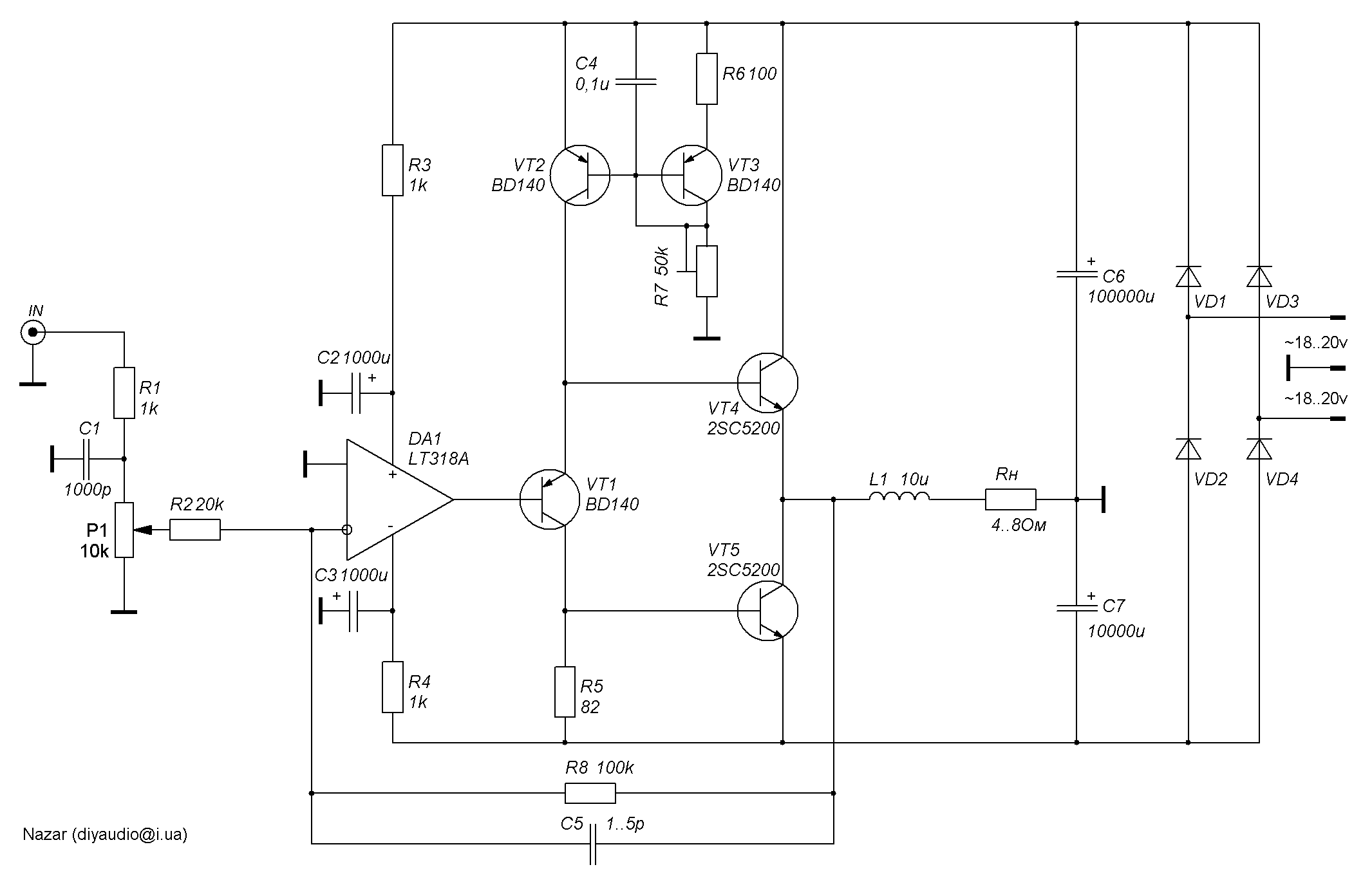
Single-Ended Current-feedback (in audio band) converter I/V
Most parallel DAC has current output. Therefore, there is a problem - how to convert current to voltage, ideally without distortion? Today mainly use two methods: the classic - at the Shelter, the resistor.
At first glance, the resistor converter option is ideal (Ohm's law), but in reality it has drawbacks. DAC to provide their passport details should work on zero input impedance converter I / U. When non-zero input impedance I / U Keys DAC external voltage is applied steady voltage drop across the resistor I / U which in turn worsens the HP DAC. With low resistance resistor resultant voltage will be very small (20-50mV) and there is another problem - how to enhance the signal quality to the desired level?
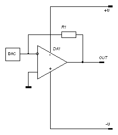
Option converter I / U on the OS (Fig. 1) is a classic, it can be found in any book on the circuit design, but it is ideal only if the ideal (ie not being implemented in practice) OS. To work as an I / U op amp must operate in a mode without limiting the rate of voltage change (intermodulyatsiynih not to introduce distortion), and also have a zero input impedance over a wide bandwidth. These conditions are not fully satisfied for any ETA running voltage or Current Feedback for ETA. Input impedance at RF in both species is inductive by reducing the RF gain, as well as (for Current Feedback OP) because the stage with common base HF has inductive input impedance before coverage DUS. The best types of Current Feedback Op Amps provide the rate of change of the output voltage 1000 - 5000V/mks, really need to choose Current Feedback Op Amps with a maximum input current to a push-pull structure despite the front end as long as possible in the class A, otherwise they will reach a steep front in AB mode ( will only work one half UN) with all the consequences ...
But apart from these two, there are other ways, such as transformer (which resale zashuntovana resistor), the transistor included in the common base (Fig. 2). Option converter I / U with transistor ON is very simple, just 4 resistors and one transistor, but it has disadvantages such as non-zero input impedance drift "zero", a relatively large output resistance and lack of linearity. But these flaws can be corrected.

The scheme proposed single-cycle current-voltage converter (Fig. 3) consists of an input stage and the output of the voltage follower. The input stage - with a common base transistor VT2. Transistor VT1 VT2 sets the offset for the zero potential for the emitter VT2 (DAC output). VT2 collector current reflects current mirror VT5, VT6, VT7 sings the collector current changes and VT1 VT2 are identical (PIC), which in turn provides a theoretically zero input impedance of this stage. Constant current generator created on the basis of the current mirror VT8, VT9 sets the initial bias current for VT2. To provide a "zero" on the emitter VT2 (DAC output) Used cascode switch VT1, VT2, which allows to equalize power allocated to them and accordingly the temperature of their crystals. Output voltage follower based on a modified cascade common-collector load as an active power source, it can significantly reduce the distortion of this stage, as well as increase the ability nagruzuchnuyu (minimum load resistance 1k).
Both cascade at low frequencies covered by the current feedback (Current-feedback) through R1, thus reducing the output impedance, and reduce distortion inverter I / U in general. At high frequencies, the feedback input stage covered only through the filter capacitor C2.
Capacitor C1 200-2000 pF capacitance reduces the input impedance of the transducer at high frequencies (10 MHz and above). Capacitor C3 prevents self-oscillation of the input stage. Inductance L1 is a ferrite bead, it prevents interference from RF output in terms of the feedback transducer. Instead, you can put a resistor L1 50-200 ohms, but its impact on the sound quality will be significant. If you change the resistor R1 feedback must be recalculated capacitance C2. Resistors R2, R3, R4, R6, R7, R8, R9 are designed to reduce the effect of Earley (dependence of the collector current of the emitter-collector voltage). Elements VT14, R12, R13, R14 are set in the case of using the DAC TDA1540, TDA1541, TDA1541A (/ R1, / S1, / S2). "Zero" at the inverter output (emitter VT13) exhibited by changing the resistor R7 (or R6) within a small range (10 - 40 ohms). In the case of TDA1540, TDA1541, TDA1541A (/ R1, / S1, / S2) "zero" exhibited by changing the resistor R14. For best results, you must choose the current mirror transistors VT5, VT6, VT7 also VT8, VT9 and VT10, VT11. BC547 transistors can be replaced by BC550, 2SC2240. BC557 transistors can be replaced by BC560, 2SA970. BF246 transistor can be replaced by any FET with an n-channel (or counting the value of resistors R13, R14). Capacitors C1, C2, C3 should be of the highest quality (the foil polypropylene, polystyrene). Resistors R1, R8, R9, R10 coal (Riken Ohm, Ohmite Little Demon, Ohmite Little Rebel, Allen Bradley, etc.) Or tantalum or qualitative metallofolgovye.
Good luck and good sound!
Literature:
1) M. Hawksford "Current-steering transimpedance amplifiers for high-resolution digital-to-analogue converters", 109th AES Convention, Los Angeles, September 2000
2) E.Barnes "Current feedback amplifiers" Analog dialogue 30-3, 30-4
3) I.Dostal "Operational Amplifiers" Moscow "Mir" 1982r.
4) P. Horowitz, U.Hill "Art circuitry" Moscow "Mir" 1998r.
5) Marcinkevi?ius, Bagdanskis "Speed ??ICs DAC and ADC and measuring their parameters" Moscow 1988r.Comment
-
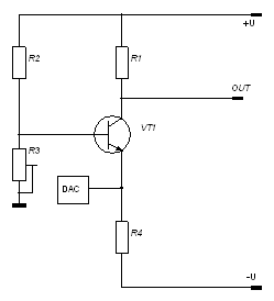
In the class A amplifier with EPD
Psevdoodnotaktny output stage, power depends on the quiescent current curves. cascade at 2A 20W gives good sound .. 4 8Oma acoustics.
Instead BD140 (Philips only) may use 2SA1837, instead 2SC5200 - 2SC3281, MJL3281A, MJL21194.
VT3 should be on the same heatsink with VT4 or VT5. With R7 set the quiescent current of the output stage.
Comment
-
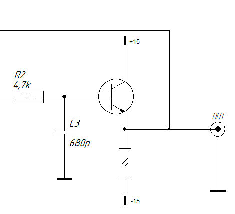
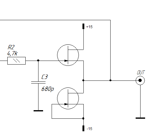
ทำไมเค้าถึงใช้ low pass ครับComment
-
ไดอะแกรมการทำงานชิบDAC เอ้าท์พุทแบบแรงดัน : DAC Analog out > Low-pass Filter
ไดอะแกรมการทำงานชิบDAC เอ้าท์พุทแบบกระแส : DAC Analog out > I/V Converter > Low-pass Filter
ตัวสุดท้ายเป็นlow-passอยู่แล้วครับ (แต่เคยเห็นบางคนบางวงจรก็ตัดวงจรส่วนนี้ออก) เพื่อตัดพวกความถี่ในช่วงที่ไม่ต้องการออกไป
[ Low-pass Filter หลายคนเรียกเพี้ยนเป็นbuffer ]
 Last edited by keang; 4 May 2014, 13:57:45.
Comment
-
ขอบคุณครัีบพี่
ลองตัดเล่น 4k7 680PF ได้มาราวๆ 50Khz(49823.4hz)


http://www.justradios.com/uFnFpF.htmlLast edited by tiger X-fi; 4 May 2014, 14:06:11.Comment
-
คืนก่อนไฟดับกลางดึก ตื่นเช้ามาเห็นคอมปิดตัวเอง เจอฟ้องเด้งเข้าหน้าrecovery bios กดข้ามไปก็ใช้งานได้ปกติ ก็ไม่ได้สนใจไรต่อ
(คอมผมไม่เคยปิด จะปิดก็เฉพาะตอนปิดร้านเที่ยวตจว.หลายวัน)
เมื่อคืนเปิดหนังดูก่อนนอน เจออาการHDAVเสียงออกข้างเดียว (นึกในใจ งานเข้าละ ท่าทาง2111SMเดี้ยงแล้วมั้ง) แต่ดึกแล้วขี้เกียจทำไร ไว้ตอนเช้าค่อยดู
วันนี้ถอดการ์ดออกมาเช็ค มันก็ปกติ มีสัญญาณปกติตั้งแต่หลังชิบDAC
ท่าทางออปแอมป์จะเดี้ยงยกชุดละมั้ง ถอดเปลี่ยนใหม่ยกชุด ก็ยังเสียงออกข้างเดียวเหมือนเดิม เอาละสิ..มันเป็นไรหว่า
สุดท้าย ลองถอดไดร์เวอร์ออกแล้วลงใหม่ ทีนี้เสียงมาครบปกติทุกอย่าง
เฮ้อออ...เล่นเอาเซ็งComment

Comment