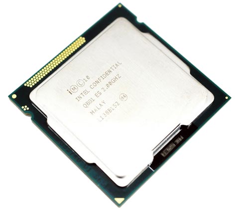
With eager OEMs such as ASUSTek, HP, Acer, and Lenovo breathing down its neck, Intel is reportedly pulling forward the official launch date of its 3rd Generation Core processor family based on 22 nm "Ivy Bridge" silicon, to the 23rd of April, from its older date of 29th April. 23rd April will be the...
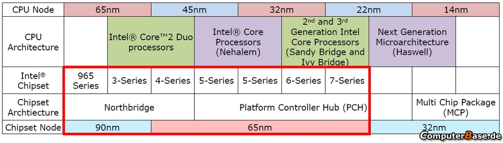
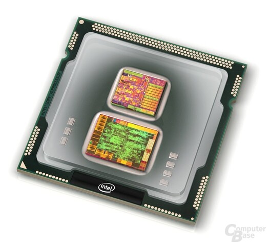
With the 14 nm "Broadwell" architecture, Intel will take a new step towards integration of the platform-controller hub (PCH) with the CPU, by designing it to be a multi-chip module (with the CPU+northbridge in one die, and PCH on the other). This would make "Broadwell" a true System-on-chip (SoC), which allows over 90 percent of the system's I/O to be routed to the processor socket, including memory, PCI-Express, SATA, USB, etc. Although not the first to the industry with single-chip chipsets and integrated memory controllers, Intel rapidly reshaped the arrangement between CPU and core-logic, over the past four years.
It began with transfer of memory controller from northbridge to CPU die (45 nm "Bloomfield"), and transfer of the entire northbridge to the CPU die (45 nm "Lynnfield"). The graphics northbridge transferred a little more gradually, first as multi-chip module with a separate CPU die (32 nm "Clarkdale"), then complete integration with the CPU die (32 nm "Sandy Bridge"). All through, the southbridge, or I/O controller hub (ICH) remained outside the CPU package, with the addition of a display output logic, it transformed into a "platform controller hub" (PCH), which is still just a glorified southbridge. Naturally then, such a drastic relocation of system components will warrant a socket change.
 Tweet
Tweet


Comment