 Tweet
Tweet
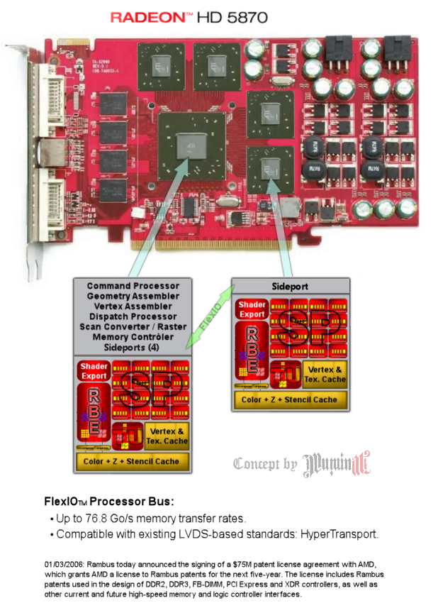
Concept -> 1 master chip and up to 4 slave chips.
The master chip is like a normal GPU... but with 4 SidePorts.
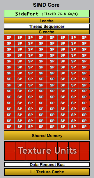
These SidePorts use the Rambus FlexIO Interface:
· Rambus FlexIO is capable of running from 400 MHz to 8 GHz.
· Contains only 12 lanes (5 lanes are inbound, 7 outbound)
· Theoretical peak I/O bandwidth of 76.8 GB @ 8 GHz (44.8GB out, 32GB in)
· Total bandwidth: 76.8GB/s x 5 SIMD Core (1 internal + 4 "slave chips") = 384GB/s
"While Cell’s XDR interface offers over 2x the memory bandwidth of any PC-based microprocsesor, Cell’s FlexIO interface weighs in at 76.8GB/s - almost 10x the chip-to-chip bandwidth of AMD’s Athlon 64." - Anandtech
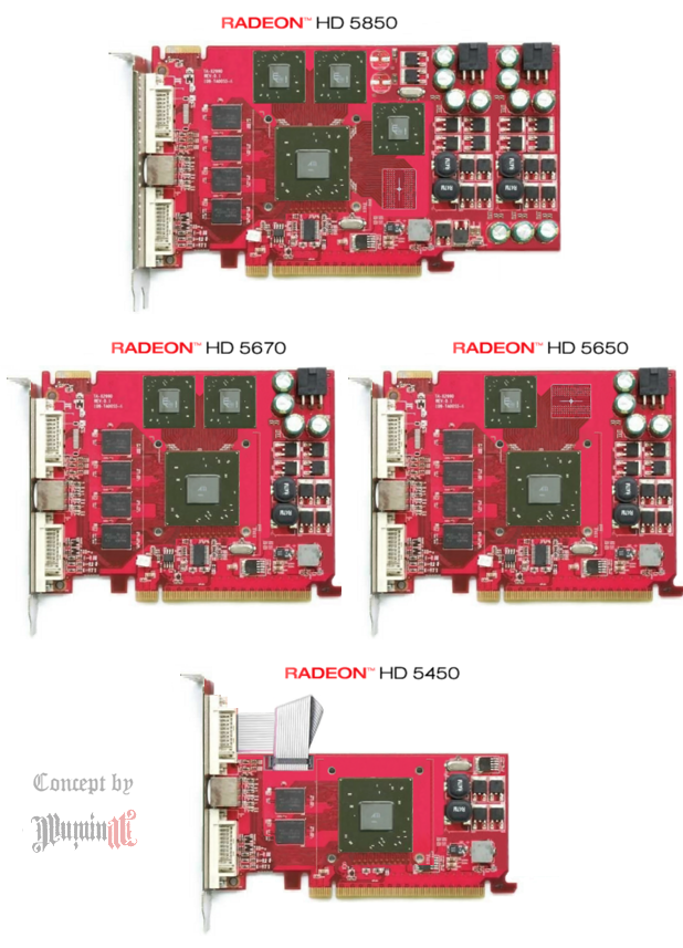
HD 5450 -> 640 SP + 16 TMUs (1 master chip)
HD 5650 -> 1280 SP + 32 TMUs (1 master chip + 1 slave)
HD 5670 -> 1920 SP + 48 TMUs (1 master chip + 2 slaves)
HD 5850 -> 2560 SP + 64 TMUs (1 master chip + 3 slaves)
HD 5870 -> 3200 SP + 80 TMUs (1 master chip + 4 slaves)
Good!:
· Need only 2 chips (master/slave) to create a complete series of graphic cards.
· The slave chip is an exact copy of the "SP/TMUs" part of the master chip.
So when you create the master chip, you also create 95% of the slave chip.
· Less time/money needed to create a new series -> 9 month product cycle instead of 12 months.
· Very small chips -> very good yields -> very good price.
· Shared memory architecture !
Bad!:
· The highest memory bandwidth hogs are the ROPs and the Level 2 texture caches, so ATI has physically placed these units next to the memory controllers and used a thousand or so traces to connect them. So, for now, it's impossible to put the RBEs inside the slave chips. Thus, the master chip has to contain enough RBEs for the HD 5870... but this high number of RBEs will be overkill for the HD 54xx/56xx. This is perhaps the major problem with this design.
เครดิต http://www.laozaa.com ครับ
ผมว่าการ์ดมันสั้นจังนะ เหอๆ
The master chip is like a normal GPU... but with 4 SidePorts.
These SidePorts use the Rambus FlexIO Interface:
· Rambus FlexIO is capable of running from 400 MHz to 8 GHz.
· Contains only 12 lanes (5 lanes are inbound, 7 outbound)
· Theoretical peak I/O bandwidth of 76.8 GB @ 8 GHz (44.8GB out, 32GB in)
· Total bandwidth: 76.8GB/s x 5 SIMD Core (1 internal + 4 "slave chips") = 384GB/s
"While Cell’s XDR interface offers over 2x the memory bandwidth of any PC-based microprocsesor, Cell’s FlexIO interface weighs in at 76.8GB/s - almost 10x the chip-to-chip bandwidth of AMD’s Athlon 64." - Anandtech
HD 5450 -> 640 SP + 16 TMUs (1 master chip)
HD 5650 -> 1280 SP + 32 TMUs (1 master chip + 1 slave)
HD 5670 -> 1920 SP + 48 TMUs (1 master chip + 2 slaves)
HD 5850 -> 2560 SP + 64 TMUs (1 master chip + 3 slaves)
HD 5870 -> 3200 SP + 80 TMUs (1 master chip + 4 slaves)
Good!:
· Need only 2 chips (master/slave) to create a complete series of graphic cards.
· The slave chip is an exact copy of the "SP/TMUs" part of the master chip.
So when you create the master chip, you also create 95% of the slave chip.
· Less time/money needed to create a new series -> 9 month product cycle instead of 12 months.
· Very small chips -> very good yields -> very good price.
· Shared memory architecture !
Bad!:
· The highest memory bandwidth hogs are the ROPs and the Level 2 texture caches, so ATI has physically placed these units next to the memory controllers and used a thousand or so traces to connect them. So, for now, it's impossible to put the RBEs inside the slave chips. Thus, the master chip has to contain enough RBEs for the HD 5870... but this high number of RBEs will be overkill for the HD 54xx/56xx. This is perhaps the major problem with this design.
เครดิต http://www.laozaa.com ครับ
ผมว่าการ์ดมันสั้นจังนะ เหอๆ
Comment